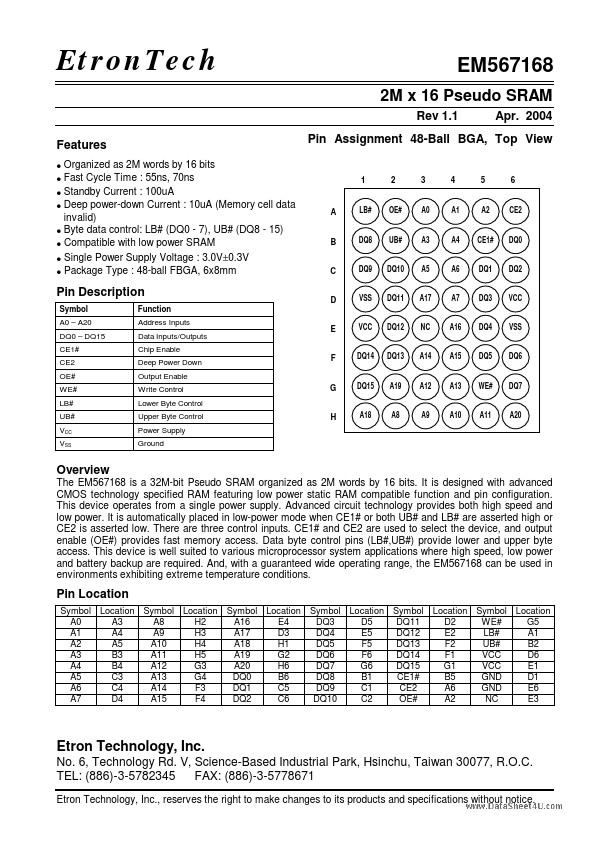
Symbol A0
A20 DQ0
DQ15 CE1# CE2 OE# WE# LB# UB# VCC VSS Function Address Inputs Data Inputs/Outputs Chip Enable Deep Power Down Output Enable Write Control Lower Byte Control Upper Byte Control Power Supply Ground
D
VSS
DQ11
A17
A7
DQ3
VCC
E
VCC
DQ12
NC
A16
DQ4
VSS
Key Features
Organized as 2M words by 16 bits.
Fast Cycle Time : 55ns, 70ns.
Standby Current : 100uA.
Deep power-down Current : 10uA (Memory cell data invalid).
Byte data control: LB# (DQ0 - 7), UB# (DQ8 - 15).
Compatible with low power SRAM.
Single Power Supply Voltage : 3.0V±0.3V.
Package Type : 48-ball FBGA, 6x8mm
EM567168
2M x 16 Pseudo SRAM
Rev 1.1 Apr. 2004 Pin Assignment 48-Ball BGA, Top View
1
2
3
4
5
6
A
LB#
OE#
A0.
Full PDF Text Transcription for EM567168 (Reference)
Note: Below is a high-fidelity text extraction (approx. 800 characters) for
EM567168. For precise diagrams, and layout, please refer to the original PDF.
EtronTech Features • Organized as 2M words by 16 bits • Fast Cycle Time : 55ns, 70ns • Standby Current : 100uA • Deep power-down Current : 10uA (Memory cell data invalid)...
View more extracted text
nt : 100uA • Deep power-down Current : 10uA (Memory cell data invalid) • Byte data control: LB# (DQ0 - 7), UB# (DQ8 - 15) • Compatible with low power SRAM • Single Power Supply Voltage : 3.0V±0.3V • Package Type : 48-ball FBGA, 6x8mm EM567168 2M x 16 Pseudo SRAM Rev 1.1 Apr.