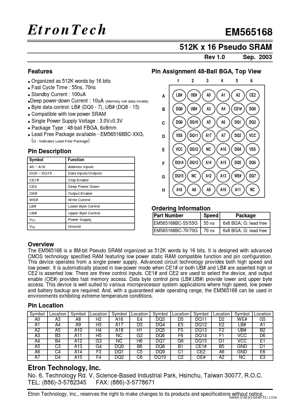
Symbol A0
A18 DQ0
DQ15 CE1# CE2 OE# WE# LB# UB# VCC VSS Function Address Inputs Data Inputs/Outputs Chip Enable Deep Power Down Output Enable Write Control Lower Byte Control Upper Byte Control Power Supply Ground
E
VCC DQ14
DQ12 DQ13
NC A14
A16 A15
DQ4 DQ5
VSS DQ6
F
G H
Key Features
Organized as 512K words by 16 bits.
Fast Cycle Time : 55ns, 70ns.
Standby Current : 100uA.
Deep power-down Current : 10uA (Memory cell data invalid).
Byte data control: LB# (DQ0 - 7), UB# (DQ8 - 15).
Compatible with low power SRAM.
Single Power Supply Voltage : 3.0V±0.3V.
Package Type : 48-ball FBGA, 6x8mm.
Lead Free Package available - EM565168BC-XXG, (G : indicates Lead Free Package)
EM565168
512K x 16 Pseudo SRA.
Full PDF Text Transcription for EM565168 (Reference)
Note: Below is a high-fidelity text extraction (approx. 800 characters) for
EM565168. For precise diagrams, and layout, please refer to the original PDF.
EtronTech Rev 1.0 Features • Organized as 512K words by 16 bits • Fast Cycle Time : 55ns, 70ns • Standby Current : 100uA •Deep power-down Current : 10uA (Memory cell data...
View more extracted text
ndby Current : 100uA •Deep power-down Current : 10uA (Memory cell data invalid) • Byte data control: LB# (DQ0 - 7), UB# (DQ8 - 15) • Compatible with low power SRAM • Single Power Supply Voltage : 3.0V±0.3V • Package Type : 48-ball FBGA, 6x8mm • Lead Free Package available - EM565168BC-XXG, (G : indicates Lead Free Package) EM565168 512K x 16 Pseudo SRAM Sep.