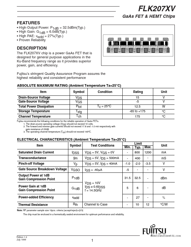
FLK207XV
FLK207XV is GaAs FET & HEMT Chips manufactured by Eudyna Devices.
FEATURES
- .. High Output Power: P1d B = 32.5d Bm(Typ.)
- High Gain: G1d B = 6.0d B(Typ.)
- High PAE: ηadd = 27%(Typ.)
- Proven Reliability
Drain
Drain
Drain
Drain
DESCRIPTION
The FLK207XV chip is a power Ga As FET that is designed for general purpose applications in the Ku-Band frequency range as it provides superior power, gain, and efficiency. Fujitsu’s stringent Quality Assurance Program assures the highest reliability and consistent performance ABSOLUTE MAXIMUM RATING (Ambient Temperature Ta=25°C)
Item Drain-Source Voltage Gate-Source Voltage Total Power Dissipation Storage Temperature Channel Temperature Symbol VDS VGS Ptot Tstg Tch Condition Rating 15 -5 Tc = 25°C 12.5 -65 to +175 175 Unit V V W °C °C
Gate Gate Gate
Fujitsu remends the following conditions for the reliable operation of Ga As FETs: 1. The drain-source operating voltage (VDS) should not exceed 10 volts. 2. The forward and reverse gate currents should not exceed 17.8 and -1.0 m A respectively with gate resistance of 250Ω. 3. The operating channel temperature (Tch) should not exceed 145°C.
ELECTRICAL CHARACTERISTICS (Ambient Temperature Ta=25°C)
Item Saturated Drain Current Transconductance Pinch-off Voltage Gate Source Breakdown Voltage Output Power at 1d B Gain pression Point Power Gain at 1d B Gain pression Point Power-added Efficiency Thermal Resistance Symbol IDSS gm Vp VGSO P1d B G1d B ηadd Rth Channel to Case VDS = 10V IDS ≈ 0.6IDSS f = 14.5GHz Test Conditions VDS = 5V, VGS = 0V VDS = 5V, IDS = 500m A VDS = 5V, IDS = 40m A IGS = -40µA Min. -1.0 -5 31.5 5 Limit Typ. Max. 800 400 -2.0 32.5 6 27 10 1200 -3.5 12 Unit m A m S V V d Bm d B % °C/W
Note: RF parameter sample size 10pcs. criteria (accept/reject)=(2/3) The chip must be enclosed in a hermetically sealed environment for optimum performance and reliability.
Edition 1.3 July 1999
Ga As FET & HEMT Chips
.. POWER
DERATING CURVE 1000
DRAIN CURRENT vs. DRAIN-SOURCE VOLTAGE
Total Power Dissipation (W)
Drain Current (m A)
16 12 8...