
Datasheet Summary
.. xr
FEBRUARY 2006
PRELIMINARY
REV. P1.0.0
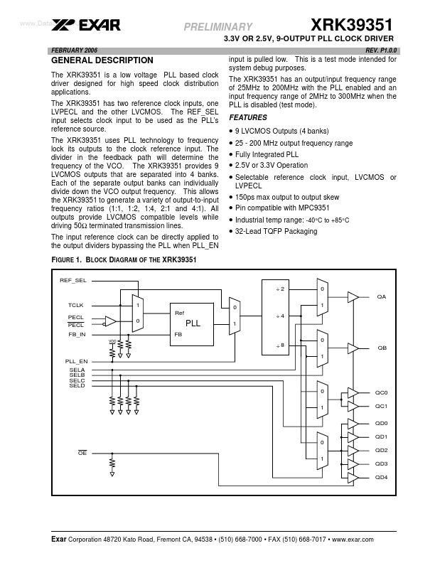
3.3V OR 2.5V, 9-OUTPUT PLL CLOCK DRIVER input is pulled low. This is a test mode intended for system debug purposes. The XRK39351 has an output/input frequency range of 25MHz to 200MHz with the PLL enabled and an input frequency range of 2MHz to 300MHz when the PLL is disabled (test mode). Features
GENERAL DESCRIPTION
The XRK39351 is a low voltage PLL based clock driver designed for high speed clock distribution applications. The XRK39351 has two reference clock inputs, one LVPECL and the other LVCMOS. The REF_SEL input selects clock input to be used as the PLL’s reference source. The XRK39351 uses PLL technology to...