Datasheet Details
| Part number | EMB07N03VQ |
|---|---|
| Manufacturer | Excelliance MOS |
| File Size | 442.47 KB |
| Description | Single N-Channel Logic Level Enhancement Mode Field Effect Transistor |
| Datasheet |
|
|
|
|
| Part number | EMB07N03VQ |
|---|---|
| Manufacturer | Excelliance MOS |
| File Size | 442.47 KB |
| Description | Single N-Channel Logic Level Enhancement Mode Field Effect Transistor |
| Datasheet |
|
|
|
|
: N-CH BVDSS 30 V RDSON (MAX.)@VGS=10V RDSON (MAX.)@VGS=4.5V 7.8 mΩ 10.5 mΩ ID @TC=25℃ 73 A Single N Channel MOSFET UIS, Rg 100% Tested Pb-Free Lead Plating & Halogen Free ▪ABSOLUTE MAXIMUM RATINGS (TC = 25 °C Unless Otherwise Noted) PARAMETERS/TEST CONDITIONS SYMBOL LIMITS Gate-Source Voltage VGS ±20 Continuous Drain Current TC = 25 °C TC = 100 °C ID 73 49 Continuous Drain Current Pulsed Drain Current1 TA = 25 °C TA = 70 °C ID 12 10 IDM 131 Avalanche Current Avalanche Energy Repetitive Avalanche Energy2 L = 0.1mH L = 0.05mH IAS 35 EAS 61 EAR 31 Power Dissipation TC = 25 °C TC = 100 °C PD 83.3 33.3 Power Dissipation TA = 25 °C TA = 70 °C PD 2.3 1.5 Operating Junction & Storage Temperature Range Tj, Tstg -55 to 150 ▪100% UIS testing in condition of VD=25V, L=0.1mH, VG=10V, IL=22A, Rated VDS=30V N-CH UNIT V A mJ W W °C ▪THERMAL RESISTANCE RATINGS THERMAL RESISTANCE Junction-to-Case Junction-to-Ambient3 SYMBOL RθJC RθJA TYPICAL 1Pulse width limited by maximum junction temperature.
2Duty cycle < 1% 355°C / W when mounted on a 1 in2 pad of 2 oz copper.
4Guarantee by Engineering test MAXIMUM 1.5 55 UNIT °C/W 2020/4/10 P.1 A.0 EMB07N03VQ ▪ELECTRICAL CHARACTERISTICS (TJ = 25 °C, Unless Otherwise Noted) PARAMETER SYMBOL TEST CONDITIONS MIN STATIC Drain-Source Breakdown Voltage4 Gate Threshold Voltage4 Gate-Body Leakage4 Zero Gate Voltage Drain Current4 On-State Drain Current1 Drain-Source On-State Resistance1,4 V(BR)DSS VGS(th) IGSS IDSS ID(ON) RDS(ON) VGS = 0V, ID = 250uA 30 VDS = VGS, ID = 250uA 1.2 VDS = 0V, VGS = ±20V VDS = 30V, VGS = 0V VDS = 30V, VGS = 0V, TJ = 125 °C VDS = 10V, VGS = 10V 73 VGS = 10V, ID = 14A VGS = 4.5V, ID = 10A DYNAMIC Input Capacitance5 Output Capacitance5 Reverse Transfer Capacitance5 Gate Resistance4,5 Total Gate Charge1,2,5 Gate-Source Charge1,2,5 Gate-
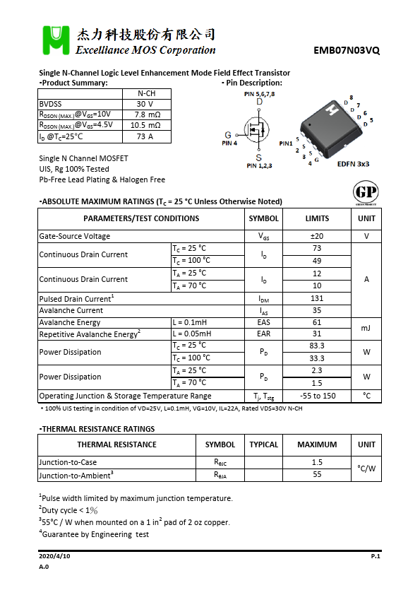
EMB07N03VQ Single N-Channel Logic Level Enhancement Mode Field Effect Transistor ▪Product Summary: ▪.
| Part Number | Description |
|---|---|
| EMB07N03V | N-Channel Logic Level Enhancement Mode Field Effect Transistor |
| EMB07N03A | N-Channel Logic Level Enhancement Mode Field Effect Transistor |
| EMB07N03HQ | N-Channel Logic Level Enhancement Mode Field Effect Transistor |
| EMB07N03HR | N-Channel Logic Level Enhancement Mode Field Effect Transistor |
| EMB07N03HS | Single N-Channel Logic Level Enhancement Mode Field Effect Transistor |
| EMB07N04A | MOSFET |
| EMB07N04H | MOSFET |
| EMB07B03H | Dual P-Channel Logic Level Enhancement Mode Field Effect Transistor |
| EMB07P03A | P-Channel Logic Level Enhancement Mode Field Effect Transistor |
| EMB07P03CS | P-Channel Logic Level Enhancement Mode Field Effect Transistor |