74LVTH32374
74LVTH32374 is Low Voltage 32-Bit D-Type Flip-Flop manufactured by Fairchild Semiconductor.
- Part of the 74LVT32374 comparator family.
- Part of the 74LVT32374 comparator family.
Description
The LVT32374 and LVTH32374 contain thirty-two noninverting D-type flip-flops with 3-STATE outputs and are intended for bus oriented applications. The device is byte controlled. A buffered clock (CP) and Output Enable (OE) are mon to each byte and can be shorted together for full 32-bit operation. The LVTH32374 data inputs include bushold, eliminating the need for external pull-up resistors to hold unused inputs. These flip-flops are designed for low-voltage (3.3V) VCC applications, but with the capability to provide a TTL interface to a 5V environment. The LVT32374 and LVTH32374 are fabricated with an advanced Bi CMOS technology to achieve high speed operation similar to 5V ABT while maintaining a low power dissipation.
Features s Input and output interface capability to systems at 5V VCC s Bushold data inputs eliminate the need for external pull-up resistors to hold unused inputs (74LVTH32374) s Also available without bushold feature
(74LVT32374) s Live insertion/extraction permitted s Power Up/Down high impedance provides glitch-free bus loading s Outputs source/sink
- 32 m A/+64 m A s ESD performance: Human-body model > 2000V Machine model > 200V Charged-device model > 1000V s Packaged in plastic Fine-Pitch Ball Grid Array (FBGA)
Ordering Code:
Order Number 74LVT32374G (Note 1)(Note 2) 74LVTH32374G (Note 1)(Note 2) Package Number BGA96A (Preliminary) BGA96A Package Description
96-Ball Fine-Pitch Ball Grid Array (FBGA), JEDEC MO-205, 5.5mm Wide 96-Ball Fine-Pitch Ball Grid Array (FBGA), JEDEC MO-205, 5.5mm Wide
Note 1: Ordering code “G” indicates Trays. Note 2: Devices also available in Tape and Reel. Specify by appending the suffix letter “X” to the ordering code.
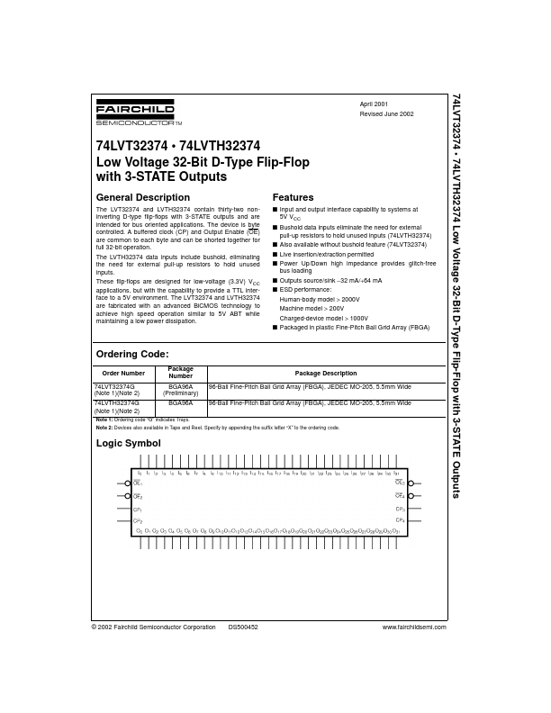
Logic Symbol
© 2002 Fairchild Semiconductor Corporation
DS500452
.fairchildsemi.
74LVT32374
- 74LVTH32374
Connection Diagram
Pin Descriptions
Pin Names OEn CPn I0- I31 O0- O31 Description
Output Enable Input (Active LOW) Clock Pulse Input Inputs 3-STATE Outputs
FBGA Pin Assignments
1 A...