Overview
- Low On-Resistance
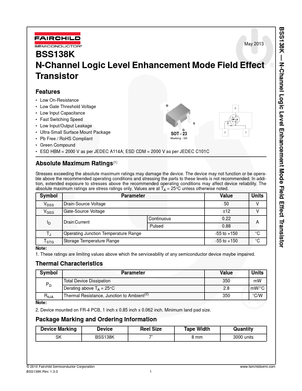
- Low Gate Threshold Voltage D
- Low Input Capacitance
- Fast Switching Speed
- Low Input/Output Leakage
- Ultra-Small Surface Mount Package
- Pb Free / RoHS Compliant G SOT - 23 Marking : SK S
- Green Compound
- ESD HBM = 2000 V as per JEDEC A114A; ESD CDM = 2000 V as per JEDEC C101C
Datasheets by Manufacturer
- BSS138K — Diodes Incorporated — 50V N-CHANNEL ENHANCEMENT MODE MOSFET
- BSS138 — Micro Commercial Components — N-Channel MOSFET
- BSS138 — onsemi — N-Channel MOSFET
- BSS138AKA — Nexperia — N-channel MOSFET
- BSS138W — onsemi — N-Channel FET
- BSS138 — H&M Semiconductor — N-Channel 50-V(D-S) MOSFET
- BSS138DW — Diodes Incorporated — DUAL N-CHANNEL MOSFET
- BSS138N — Analog Power — N-Channel MOSFET
- BSS138PS — NXP Semiconductors — MOSFET
- BSS138BK — Nexperia — N-channel MOSFET