Datasheet Details
| Part number | FDB2614 |
|---|---|
| Manufacturer | Fairchild (now onsemi) |
| File Size | 0.99 MB |
| Description | N-Channel MOSFET |
| Datasheet | FDB2614_FairchildSemiconductor.pdf |
|
|
|
Overview: FDB2614 — N-Channel PowerTrench® MOSFET November 2013 FDB2614 N-Channel PowerTrench® MOSFET 200 V, 62 A, 27.
| Part number | FDB2614 |
|---|---|
| Manufacturer | Fairchild (now onsemi) |
| File Size | 0.99 MB |
| Description | N-Channel MOSFET |
| Datasheet | FDB2614_FairchildSemiconductor.pdf |
|
|
|
This N-Channel MOSFET is producedusing Fairchild Semiconductor’s advanced PowerTrench® process that has been tailored to minimize the on-state resistance while maintaining superior switching performance.
Applications • Synchronous Rectification • Battery Protection Circuit • Motor Drives and Uninterruptible Power Supplies
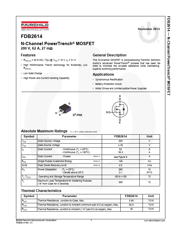
 D D G S D2-PAK G S Absolute Maximum Ratings TC = 25°C unless otherwise noted Symbol Parameter VDS Drain-Source Voltage VGS Gate-Source Voltage ID Drain Current - Continuous (TC = 25°C) - Continuous (TC = 100°C) IDM Drain Current - Pulsed (Note 1) EAS dv/dt PD Single Pulsed Avalanche Energy Peak Diode Recovery dv/dt Power Dissipation (TC = 25°C) - Derate above 25°C (Note 2) (Note 3) TJ, TSTG TL Operating and Storage Temperature Range Maximum Lead Temperature for Soldering Purpose, 1/8” from Case for 5 Seconds FDB2614 200 ± 30 62 39.3 see Figure 9 145 4.5 260 2.1 -55 to +150 300 Thermal Characteristics Symbol Parameter RθJC RθJA RθJA Thermal Resistance, Junction-to-Case, Max.
Thermal Resistance, Junction to Ambient (minimum pad of 2 oz copper), Max.
| Part Number | Description |
|---|---|
| FDB2670 | N-Channel MOSFET |
| FDB20AN06A0 | N-Channel PowerTrench MOSFET |
| FDB24AN06LA0 | N-Channel PowerTrench MOSFET |
| FDB2532 | N-Channel MOSFET |
| FDB2532_F085 | N-Channel MOSFET |
| FDB2552 | N-Channel MOSFET |
| FDB2552_F085 | N-Channel MOSFET |
| FDB2570 | N-Channel MOSFET |
| FDB2572 | 150V 29A N-Channel MOSFET |
| FDB2710 | N-Channel MOSFET |