FDD6778A
FDD6778A is N-Channel MOSFET manufactured by Fairchild Semiconductor.
FDD6778A N-Channel Power Trench® MOSFET
January 2009
N-Channel Power Trench® MOSFET
25 V, 14.0 mΩ Features
General Description
This N-Channel MOSFET has been designed specifically to improve the overall efficiency of DC/DC converters using either synchronous or conventional switching PWM controllers. It has been optimized for low gate charge, low r DS(on) and fast switching speed.
- Max r DS(on) = 14.0 mΩ at VGS = 10 V, ID = 10.0 A
- Max r DS(on) = 30.0 mΩ at VGS = 4.5 V, ID = 9.7 A
- 100% UIL tested
- Ro HS pliant
Applications
- Vcore DC-DC for Desktop puters and Servers
- VRM for Intermediate Bus Architecture
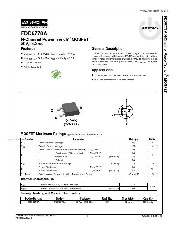
D-PAK TO -252 (TO-252)
MOSFET Maximum Ratings TC = 25 °C unless otherwise noted
.. Symbol VDS
VGS Parameter Drain to Source Voltage Gate to Source Voltage Drain Current -Continuous (Package limited) ID -Continuous (Silicon limited) -Continuous -Pulsed EAS PD TJ, TSTG Single Pulse Avalanche Energy Power Dissipation Power Dissipation TC = 25 °C TA = 25 °C (Note 1a) (Note 3) TC = 25 °C TC = 25 °C TA = 25 °C (Note 1a) Ratings 25 ±20 10 30 12 50 12 24 3.7 -55 to +175 m J W °C A Units V V
Operating and Storage Junction Temperature Range
Thermal Characteristics
RθJC RθJA Thermal Resistance, Junction to Case Thermal Resistance, Junction to Ambient (Note 1a) 6.2 40 °C/W
Package Marking and Ordering Information
Device Marking FDD6778A Device FDD6778A Package D-PAK (TO-252) Reel Size 13 ’’ Tape Width 12 mm Quantity 2500 units
©2009 Fairchild Semiconductor Corporation FDD6778A Rev.C
.fairchildsemi.
FDD6778A N-Channel Power Trench® MOSFET
Electrical Characteristics TJ = 25 °C unless otherwise noted
Symbol Parameter Test Conditions Min Typ Max Units
Off Characteristics
BVDSS ∆BVDSS ∆TJ IDSS IGSS Drain to Source Breakdown Voltage Breakdown Voltage Temperature Coefficient Zero Gate Voltage Drain Current Gate to Source Leakage Current ID = 250 µA, VGS = 0 V ID = 250 µA, referenced to 25 °C VDS = 20 V, VGS = 0 V...