FDS6812A
FDS6812A is Dual N-Channel Logic Level PWM Optimized PowerTrench MOSFET manufactured by Fairchild Semiconductor.
escription
These N-Channel Logic Level MOSFETs are produced using Fairchild Semiconductor’s advanced Power Trench process that has been especially tailored to minimize the on-state resistance and yet maintain superior switching performance. These devices are well suited for low voltage and battery powered applications where low in-line power loss and fast switching are required.
Features
- 6.7 A, 20 V. RDS(ON) = 22 mΩ @ VGS = 4.5 V RDS(ON) = 35 mΩ @ VGS = 2.5 V
- Low gate charge (12 n C typical)
- High performance trench technology for extremely low RDS(ON)
- High power and current handling capability
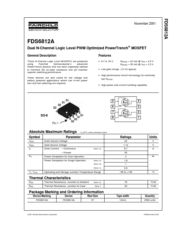
D2 D
D2 D
DD1 D1 D
5 6 7
Q1
4 3 2
Q2
SO-8
Pin 1 SO-8
G2 S2 S
G1 S1 G
Absolute Maximum Ratings
Symbol
VDSS VGSS ID PD Drain-Source Voltage Gate-Source Voltage Drain Current
- Continuous
- Pulsed
TA=25 C unless otherwise noted o
Parameter
Ratings
20 ± 12
(Note 1a)
Units
6.7 35...