FEATURES
GENERAL DESCRIPTION
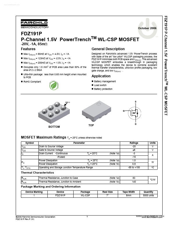
Max rDS(on) = 85mΩ at VGS = -4.5V, ID = -1A Max rDS(on) = 123mΩ at VGS = -2.5V, ID = -1A Max rDS(on) = 200mΩ at VGS = -1.5V, ID = -1A Occupies only 1.5 mm2 of PCB area Less than 50% of the area of 2 x 2 BGA Ultra-thin package: less than 0.65 mm height when mounted to PCB RoHS Compliant tm Designed on Fairchild's advanced 1.5V PowerTrench process with state of the art "low pitch" WLCSP packaging process, the FDZ191P minimizes both PCB space and rDS(on). . Application Battery management Load switch Battery protection PIN 1 S S D D S G S G BOTTOM TOP D MOSFET MAXIMUM RATINGS
TA = 25°C unless otherwise noted Symbol VDS VGS ID PD TJ, TSTG Parameter Drain to Source Voltage Gate to Source Voltage Drain Current -Continuous -Pulsed Power Dissipation Power Dissipation TA = 25°C TA = 25°C (Note 1a) (Note 1b) TA = 25°C (Note 1a) Ratings -20 ±8 -3 -15 1.5 0.9 -55 to +150 Units V V A W °C Operating and Storage Junction Temperature Range Thermal Characte... Fairchild Semiconductor