FDZ371PZ
FDZ371PZ is Thin WL-CSP MOSFET manufactured by Fairchild Semiconductor.
FDZ371PZ P-Channel 1.5 V Specified Power Trench® Thin WL-CSP MOSFET
July 2009
P-Channel 1.5 V Specified Power Trench Thin WL-CSP MOSFET
-20 V, -3.7 A, 75 mΩ
Features
- Max r DS(on) = 75 mΩ at VGS = -4.5 V, ID = -2.0 A
- Max r DS(on) = 90 mΩ at VGS = -2.5 V, ID = -1.5 A
- Max r DS(on) = 110 mΩ at VGS = -1.8 V, ID = -1.0 A
- Max r DS(on) = 150 mΩ at VGS = -1.5 V, ID = -1.0 A
- Occupies only 1.0 mm2 of PCB area.Less than 30% of the area of 2 x 2 BGA
- Ultra-thin package: less than 0.4 mm height when mounted to PCB
- HBM ESD protection level >4.4k V typical (Note 3)
- Ro HS pliant
® tm
General Description
Designed on Fairchild's advanced 1.5 V Power Trench® process with state of the art "fine pitch" Thin WLCSP packaging process, the FDZ371PZ minimizes both PCB space and r DS(on). This advanced WLCSP MOSFET embodies a breakthrough in packaging technology which enables the device to bine excellent thermal transfer characteristics, ultra-low profile packaging, low gate charge, and low r DS(on).
Applications
- Battery management
- Load switch
- Battery protection
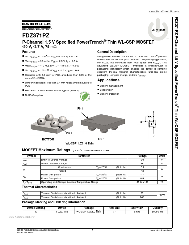
Pin 1 S D G S
Pin 1
BOTTOM WL-CSP 1.0X1.0 Thin
MOSFET Maximum Ratings TA = 25 °C unless otherwise noted
Symbol VDS VGS ID PD TJ, TSTG Parameter Drain to Source Voltage Gate to Source Voltage -Continuous -Pulsed Power Dissipation Power Dissipation TA = 25°C TA = 25°C (Note 1a) (Note 1b) TA = 25°C (Note 1a) Ratings -20 ±8 -3.7 -12 1.7 0.5 -55 to +150 Units V V A W °C
Operating and Storage Junction Temperature Range
Thermal Characteristics
RθJA RθJA Thermal Resistance, Junction to Ambient Thermal Resistance, Junction to Ambient (Note 1a) (Note 1b) 75 260 °C/W
Package Marking and Ordering Information
Device Marking K Device FDZ371PZ Package WL-CSP 1.0X1.0 Thin Reel Size 7” Tape Width 8 mm Quantity 5000...