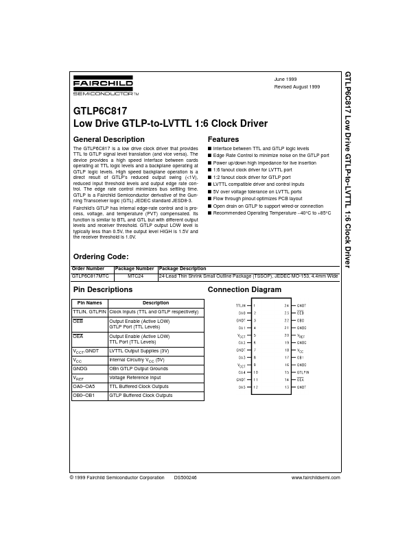
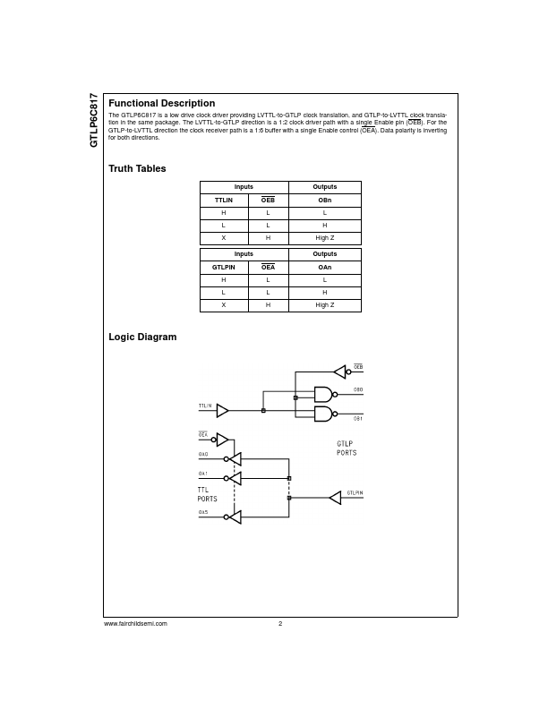
Datasheet4U Logo Datasheet4U.com

GTLP6C817 - Low Drive GTLP-to-LVTTL 1:6 Clock Driver

Description

The GTLP6C817 is a low drive clock driver that provides TTL to GTLP signal level translation (and vice versa).

The device provides a high speed interface between cards operating at TTL logic levels and a backplane operating at GTLP logic levels.

Features

  • s Interface between TTL and GTLP logic levels s Edge Rate Control to minimize noise on the GTLP port s Power up/down high impedance for live insertion s 1:6 fanout clock driver for LVTTL port s 1:2 fanout clock driver for GTLP port s LVTTL compatible driver and control inputs s 5V over voltage tolerance on LVTTL ports s Flow through pinout optimizes PCB layout s Open drain on GTLP to support wired-or connection s Recommended Operating Temperature.
  • 40°C to +85°C Ordering Code: Order Numb.

📥 Download Datasheet

Full PDF Text Transcription

Click to expand full text
GTLP6C817 Low Drive GTLP-to-LVTTL 1:6 Clock Driver June 1999 Revised August 1999 GTLP6C817 Low Drive GTLP-to-LVTTL 1:6 Clock Driver General Description The GTLP6C817 is a low drive clock driver that provides TTL to GTLP signal level translation (and vice versa). The device provides a high speed interface between cards operating at TTL logic levels and a backplane operating at GTLP logic levels. High speed backplane operation is a direct result of GTLP’s reduced output swing (<1V), reduced input threshold levels and output edge rate control. The edge rate control minimizes bus settling time. GTLP is a Fairchild Semiconductor derivative of the Gunning Transceiver logic (GTL) JEDEC standard JESD8-3.
Published: |