ISL9N7030BLS3ST
ISL9N7030BLS3ST is N-Channel Power MOSFET manufactured by Fairchild Semiconductor.
eatures low gate charge while maintaining low on-resistance. Optimized for switching applications, this device improves the overall efficiency of DC/DC converters and allows operation to higher switching frequencies.
PWM Optimized Features
- -
- -
- - Fast Switching r DS(ON) = 0.0064Ω (Typ), VGS = 10V r DS(ON) = 0.010Ω (Typ), VGS = 4.5V Qg Total 24n C (Typ), VGS = 5V Qgd (Typ)
- -
- -
- - . . . . 11n C CISS (Typ)
- -
- -
- - . 2600p F
Packaging
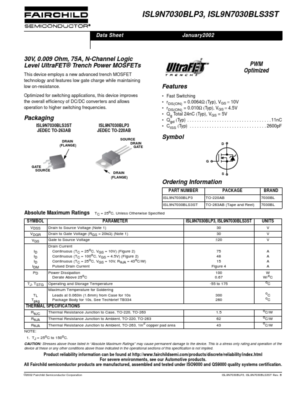
ISL9N7030BLS3ST JEDEC TO-263AB
DRAIN (FLANGE)
ISL9N7030BLP3 JEDEC TO-220AB
SOURCE DRAIN GATE
Symbol
G GATE SOURCE DRAIN (FLANGE)
Ordering Information
PART NUMBER ISL9N7030BLP3 ISL9N7030BLS3ST PACKAGE TO-220AB TO-263AB (Tape and Reel) BRAND 7030BL 7030BL
Absolute Maximum Ratings
SYMBOL VDSS VDGR VGS ID ID ID IDM PD TJ, TSTG TL Tpkg RθJC RθJA RθJA NOTE: 1. TJ = 25o C to 150o C.
TC = 25o C, Unless Otherwise Specified PARAMETER ISL9N7030BLP3, ISL9N7030BLS3ST 30 30 ±20 75 48 15 Figure 4 100 0.67 -55 to 175 300 260 1.5 62 43 UNITS V V V A A A A W W/o C o C o C o C o C/W o C/W o C/W
Drain to Source Voltage (Note 1) Drain to Gate Voltage (RGS = 20kΩ) (Note 1) Gate to Source Voltage Drain Current Continuous (TC = 25o C, VGS = 10V) (Figure 2) Continuous (TC = 100o C, VGS = 4.5V) (Figure 2) Continuous (TC = 25o C, VGS = 10V, RθJA = 43o C/W) Pulsed Drain Current Power Dissipation Derate Above 25o C Operating and Storage Temperature Maximum Temperature for Soldering Leads at 0.063in (1.6mm) from Case for 10s Package Body for 10s, See Techbrief TB334 Thermal Resistance Junction to Case, TO-220, TO-263 Thermal Resistance Junction to Ambient, TO-220, TO-263 Thermal Resistance Junction to Ambient, TO-263, 1in 2 copper pad area
THERMAL SPECIFICATIONS
CAUTION: Stresses above those listed in “Absolute Maximum Ratings” may cause permanent damage to the device. This is a stress only rating and operation of the device at these or any other conditions above...