Datasheet4U Logo Datasheet4U.com

NDS355N - N-Channel Logic Level Enhancement Mode Field Effect Transistor

General Description

These N-Channel logic level enhancement mode power field effect transistors are produced using Fairchild's proprietary, high cell density, DMOS technology.

This very high density process is especially tailored to minimize on-state resistance.

Key Features

  • 1.6A, 30V. RDS(ON) = 0.125Ω @ VGS = 4.5V. Proprietary package design using copper lead frame for superior thermal and electrical capabilities. High density cell design for extremely low RDS(ON). Exceptional on-resistance and maximum DC current capability. Compact industry standard SOT-23 surface mount package
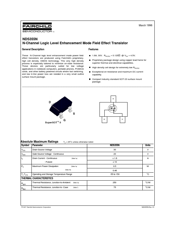
. _______________________________________________________________________________ D G S Absolute Maximum Ratings Symbol VDSS VGSS ID PD TJ,TSTG Parameter Drain-Source Voltage T A = 25°.

📥 Download Datasheet

Full PDF Text Transcription (Reference)

The following content is an automatically extracted verbatim text from the original manufacturer datasheet and is provided for reference purposes only.

View original datasheet text
March 1996 NDS355N N-Channel Logic Level Enhancement Mode Field Effect Transistor General Description These N-Channel logic level enhancement mode power field effect transistors are produced using Fairchild's proprietary, high cell density, DMOS technology. This very high density process is especially tailored to minimize on-state resistance. These devices are particularly suited for low voltage applications in notebook computers, portable phones, PCMICA cards, and other battery powered circuits where fast switching, and low in-line power loss are needed in a very small outline surface mount package. Features 1.6A, 30V. RDS(ON) = 0.125Ω @ VGS = 4.5V. Proprietary package design using copper lead frame for superior thermal and electrical capabilities.