MHVIC2114NR2
MHVIC2114NR2 is RF LDMOS Wideband Integrated Power Amplifier manufactured by Freescale Semiconductor.
Features
- Characterized with Series Equivalent Large
- Signal Impedance Parameters and mon Source Scattering Parameters
- On
- Chip Matching (50 Ohm Input, DC Blocked, >5 Ohm Output)
- Integrated Temperature pensation with Enable/Disable Function
- Integrated ESD Protection
- Ro HS pliant
- In Tape and Reel. R2 Suffix = 1,500 Units per 16 mm, 13 inch Reel.
2100 MHz, 27 V, 23 d Bm SINGLE W
- CDMA RF LDMOS WIDEBAND INTEGRATED POWER AMPLIFIER
16 1
CASE 978
- 03 PFP
- 16
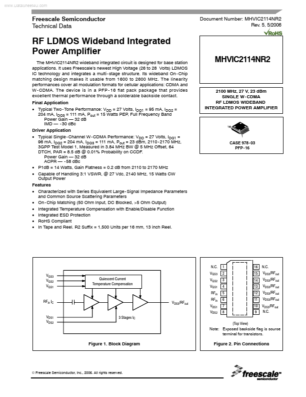
N.C. VGS3 VGS2 VGS1 VGS3 Quiescent Current Temperature pensation VGS2 VGS1 RFin RFin IC VDS3/RFout RFin VDS1 VDS2
1 2 3 4 5 6 7 8
16 15 14 13 12 11 10 9
N.C. VDS3/RFout VDS3/RFout VDS3/RFout VDS3/RFout VDS3/RFout VDS3/RFout N.C.
VDS1 VDS2
3 Stages IC (Top View) Note: Exposed backside flag is source terminal for transistors.
Figure 1. Block Diagram
Figure 2. Pin Connections
© Freescale Semiconductor, Inc., 2006. All rights reserved.
MHVIC2114NR2 1
RF Device Data Freescale Semiconductor
Table 1. Maximum Ratings
Rating Drain- Source Voltage Gate- Source Voltage Storage Temperature Range Operating Junction Temperature Input Power Symbol VDSS VGS Tstg TJ Pin Value
- 0.5, +65
- 0.5, +15
- 65 to +150 150 5 Unit Vdc Vdc °C °C d Bm
Table 2. Thermal Characteristics
Characteristic Thermal Resistance, Junction to Case Driver Application (Pout = +0.2 W CW) Stage 1, 27 Vdc, IDQ1 = 96 m A Stage 2, 27 Vdc, IDQ2 = 204 m A Stage 3, 27 Vdc, IDQ3 = 111 m A Symbol RθJC 11.5 7.52 5.52 Value Unit °C/W
Table 3. ESD Protection Characteristics
Test Methodology Human Body Model (per JESD22
- A114) Machine Model (per EIA/JESD22
- A115) Charge Device Model (per JESD22
- C101) Class 0 (Minimum) A...