MRF5P20180HR6
MRF5P20180HR6 is RF Power Field Effect Transistor manufactured by Freescale Semiconductor.
Freescale Semiconductor Technical Data
MRF5P20180HR6 Rev. 0, 12/2004
RF Power Field Effect Transistor
- Channel Enhancement
- Mode Lateral MOSFET
Designed for W- CDMA base station applications with frequencies from 1930 to 1990 MHz. Suitable for TDMA, CDMA and multicarrier amplifier applications. To be used in Class AB for PCN
- PCS/cellular radio and WLL applications.
- Typical 2
- carrier W
- CDMA Performance: VDD = 28 Volts, IDQ = 2 x 800 m A, Pout = 38 Watts Avg., Full Frequency Band, Channel Bandwidth = 3.84 MHz, Peak/Avg. = 8.5 d B @ 0.01% Probability on CCDF. Power Gain
- 14 d B Drain Efficiency
- 26% IM3 @ 10 MHz Offset
- - 37.5 d Bc @ 3.84 MHz Channel Bandwidth ACPR @ 5 MHz Offset
- - 41 d Bc @ 3.84 MHz Channel Bandwidth
- Capable of Handling 10:1 VSWR, @ 28 Vdc, 1960 MHz, 120 Watts CW Output Power
- Characterized with Series Equivalent Large
- Signal Impedance Parameters
- Internally Matched, Controlled Q, for Ease of Use
- Qualified Up to a Maximum of 32 VDD Operation
- Integrated ESD Protection
- Lower Thermal Resistance Package
- Low Gold Plating Thickness on Leads, 40µ″ Nominal.
- In Tape and Reel. R6 Suffix = 150 Units per 56 mm, 13 inch Reel.
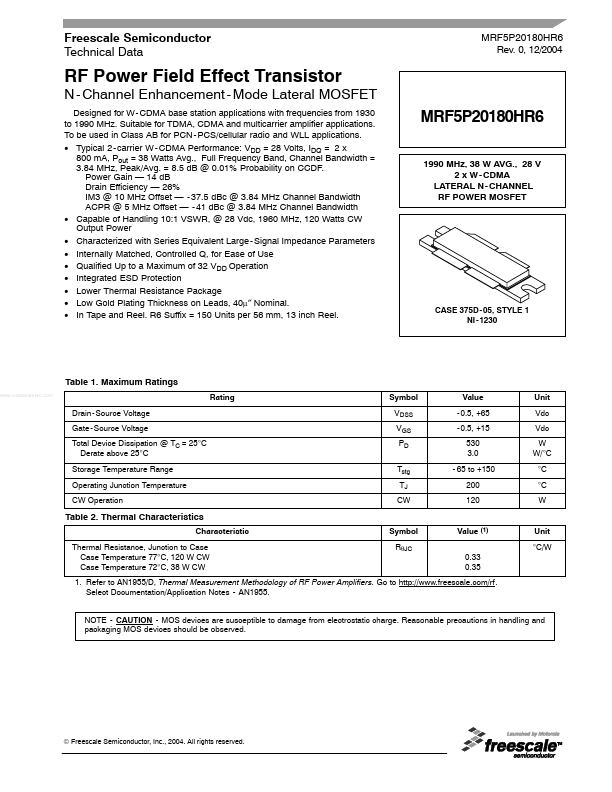
1990 MHz, 38 W AVG., 28 V 2 x W
- CDMA LATERAL N
- CHANNEL RF POWER MOSFET
CASE 375D
- 05, STYLE 1 NI
- 1230
Table 1. Maximum Ratings
..
Rating Drain
- Source Voltage Gate
- Source Voltage Total Device Dissipation @ TC = 25°C Derate above 25°C Storage Temperature Range Operating Junction Temperature CW Operation
Symbol VDSS VGS PD Tstg TJ CW
Value
- 0.5, +65
- 0.5, +15 530 3.0
- 65 to +150 200...