MRF5P21045NR1
MRF5P21045NR1 is RF Power Field-Effect Transistor N-Channel Enhancement-Mode Lateral MOSFET manufactured by Freescale Semiconductor.
Features
- Characterized with Series Equivalent Large
- Signal Impedance Parameters
- Internally Matched for Ease of Use
- Qualified Up to a Maximum of 32 VDD Operation
- Integrated ESD Protection
- 200°C Capable Plastic Package
- Ro HS pliant
- In Tape and Reel. R1 Suffix = 500 Units per 44 mm, 13 inch Reel.
- 2170 MHz, 10 W AVG., 28 V 2 x W
- CDMA, DUAL PATH LATERAL N
- CHANNEL RF POWER MOSFET
CASE 1486
- 03, STYLE 1 TO
- 270 WB
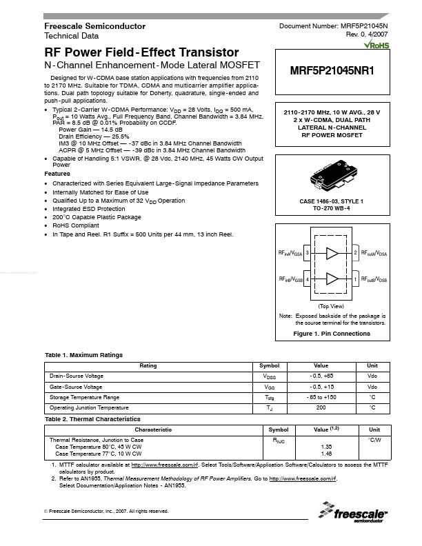
- 4
RFin A/VGSA 3
2 RFout A/VDSA
..
RFin B/VGSB 4
1 RFout B/VDSB
(Top View) Note: Exposed backside of the package is the source terminal for the transistors.
Figure 1. Pin Connections Table 1. Maximum Ratings
Rating Drain
- Source Voltage Gate
- Source Voltage Storage Temperature Range Operating Junction Temperature Symbol VDSS VGS Tstg TJ Value
- 0.5, +65
- 0.5, + 15
- 65 to +150 200 Unit Vdc Vdc °C °C
Table 2. Thermal Characteristics
Characteristic Thermal Resistance, Junction to Case Case Temperature 80°C, 45 W CW Case Temperature 77°C, 10 W CW Symbol RθJC Value (1,2) 1.35 1.48 Unit °C/W
1. MTTF calculator available at http://.freescale./rf. Select Tools/Software/Application Software/Calculators to access the MTTF calculators by product. 2. Refer to AN1955, Thermal Measurement Methodology of RF Power Amplifiers. Go to http://.freescale./rf. Select Documentation/Application Notes
- AN1955.
© Freescale Semiconductor, Inc., 2007. All rights reserved.
MRF5P21045NR1 1
RF Device Data Freescale Semiconductor
Table 3. ESD Protection Characteristics
Test Methodology Human Body Model (per JESD22
- A114) Machine Model (per EIA/JESD22
- A115) Charge Device Model (per...