MRF6S18100NBR1
MRF6S18100NBR1 is RF Power Field Effect Transistors manufactured by Freescale Semiconductor.
Freescale Semiconductor Technical Data
Document Number: MRF6S18100N Rev. 1, 5/2006
RF Power Field Effect Transistors
- Channel Enhancement
- Mode Lateral MOSFETs
Designed for GSM and GSM EDGE base station applications with frequenc ies from 1800 to 2000 MHz . S u i t a b l e f o r T D M A , C D M A a n d multicarrier amplifier applications.
..
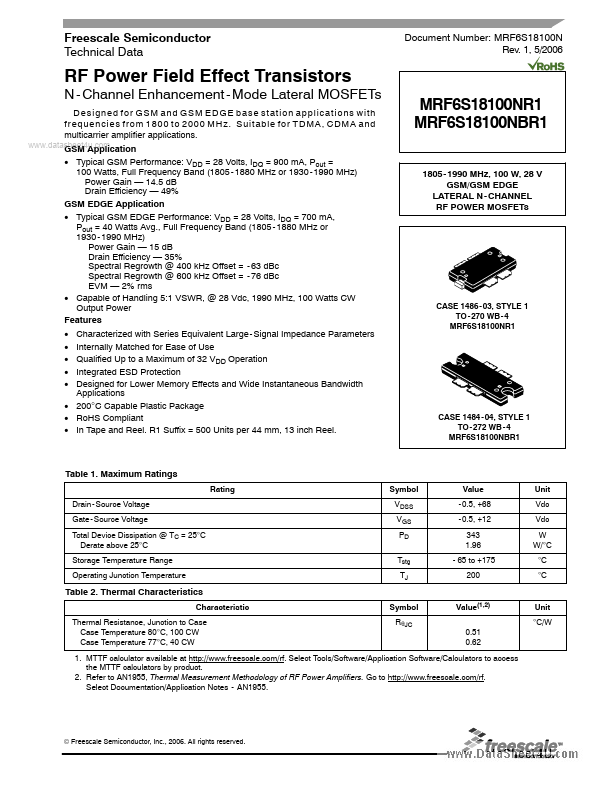
MRF6S18100NR1 MRF6S18100NBR1
1805- 1990 MHz, 100 W, 28 V GSM/GSM EDGE LATERAL N
- CHANNEL RF POWER MOSFETs
GSM Application
- Typical GSM Performance: VDD = 28 Volts, IDQ = 900 m A, Pout = 100 Watts, Full Frequency Band (1805
- 1880 MHz or 1930- 1990 MHz) Power Gain
- 14.5 d B Drain Efficiency
- 49% GSM EDGE Application
- Typical GSM EDGE Performance: VDD = 28 Volts, IDQ = 700 m A, Pout = 40 Watts Avg., Full Frequency Band (1805
- 1880 MHz or 1930- 1990 MHz) Power Gain
- 15 d B Drain Efficiency
- 35% Spectral Regrowth @ 400 k Hz Offset =
- 63 d Bc Spectral Regrowth @ 600 k Hz Offset =
- 76 d Bc EVM
- 2% rms
- Capable of Handling 5:1 VSWR, @ 28 Vdc, 1990 MHz, 100 Watts CW Output Power Features
- Characterized with Series Equivalent Large
- Signal Impedance Parameters
- Internally Matched for Ease of Use
- Qualified Up to a Maximum of 32 VDD Operation
- Integrated ESD Protection
- Designed for Lower Memory Effects and Wide Instantaneous Bandwidth Applications
- 200°C Capable Plastic...