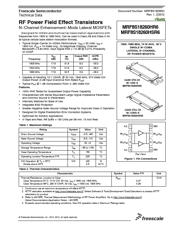
MRF8S18260HSR6
MRF8S18260HSR6 is RF Power Field Effect Transistors manufactured by Freescale Semiconductor.
- Part of the MRF8S18260HR6 comparator family.
- Part of the MRF8S18260HR6 comparator family.
Freescale Semiconductor Technical Data
Document Number: MRF8S18260H Rev. 1, 2/2012
RF Power Field Effect Transistors
N--Channel Enhancement--Mode Lateral MOSFETs
Designed for CDMA and multicarrier base station applications with frequencies from 1805 to 1880 MHz. Can be used in Class AB and Class C for all typical cellular base station modulation formats.
- 1BT6yap0ni0dcwamlidASt,ihnPg=oleu3t--.=8C4a7rM4riHWerzaW,ttIsn--pCAuDvtgMS.,iAgIQnPaeMlrPfaoAgrRnmita=und7ce.e5C: dVliBpDpD@in=g03,.00C1hV%aonltPnsre,olIDbaQb=ility on CCDF.
Frequency
Gps (dB)
ηD Output PAR ACPR
(%)
(dB)
(dBc)
1805 MHz
17.9 31.6
6.0 --35.0
1840 MHz
17.9 31.9
6.0 --36.0
1880 MHz
17.9 32.5
5.9 --36.0
-...