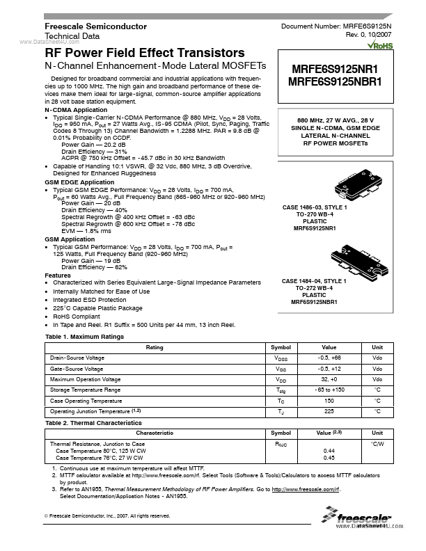
MRFE6S9125NR1
MRFE6S9125NR1 is N-Channel Enhancement-Mode Lateral MOSFETs manufactured by Freescale Semiconductor.
- Part of the MRFE6S9125NBR1 comparator family.
- Part of the MRFE6S9125NBR1 comparator family.
..
Freescale Semiconductor Technical Data
Document Number: MRFE6S9125N Rev. 0, 10/2007
RF Power Field Effect Transistors
- Channel Enhancement
- Mode Lateral MOSFETs
Designed for broadband mercial and industrial applications with frequencies up to 1000 MHz. The high gain and broadband performance of these devices make them ideal for large-signal, mon-source amplifier applications in 28 volt base station equipment. N
- CDMA Application
- Typical Single
- Carrier N
- CDMA Performance @ 880 MHz, VDD = 28 Volts, IDQ = 950 m A, Pout = 27 Watts Avg., IS
- 95 CDMA (Pilot, Sync, Paging, Traffic Codes 8 Through 13) Channel Bandwidth = 1.2288 MHz. PAR = 9.8 d B @ 0.01% Probability on CCDF. Power Gain
- 20.2 d B Drain Efficiency
- 31% ACPR @ 750 k Hz Offset =
- 45.7 d Bc in 30 k Hz Bandwidth
- Capable of Handling 10:1 VSWR, @ 32 Vdc, 880 MHz, 3 d B Overdrive, Designed for Enhanced Ruggedness GSM EDGE Application
- Typical GSM EDGE Performance: VDD = 28 Volts, IDQ = 700 m A, Pout = 60 Watts Avg., Full Frequency Band (865
- 960 MHz or 920
- 960 MHz) Power Gain
- 20 d B Drain Efficiency
- 40% Spectral Regrowth @ 400 k Hz Offset =
- 63 d Bc Spectral Regrowth @ 600 k Hz Offset =
- 78 d Bc EVM
- 1.8% rms GSM Application
- Typical GSM Performance: VDD = 28 Volts, IDQ = 700 m A, Pout = 125 Watts, Full Frequency Band (920
- 960 MHz) Power Gain
- 19 d B Drain Efficiency
- 62% Features
- Characterized with Series Equivalent Large
- Signal Impedance...