MRFE6VP5600HSR6
MRFE6VP5600HSR6 is RF Power Field Effect Transistors manufactured by Freescale Semiconductor.
- Part of the MRFE6VP5600HR6 comparator family.
- Part of the MRFE6VP5600HR6 comparator family.
.Data Sheet.co.kr
Freescale Semiconductor Technical Data
Document Number: MRFE6VP5600H Rev. 1, 1/2011
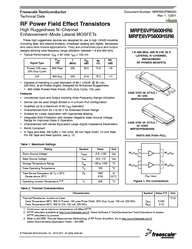
RF Power Field Effect Transistors
High Ruggedness N--Channel Enhancement--Mode Lateral MOSFETs
These high ruggedness devices are designed for use in high VSWR industrial (including laser and plasma exciters), broadcast (analog and digital), aerospace and radio/land mobile applications. They are unmatched input and output designs allowing wide frequency range utilization, between 1.8 and 600 MHz.
- Typical Performance: VDD = 50 Volts, IDQ = 100 m A
Signal Type Pulsed (100 μsec, 20% Duty Cycle) CW Pout (W) 600 Peak 600 Avg. f (MHz) 230 230 Gps (d B) 25.0 24.6 ηD (%) 74.6 75.2 IRL (d B) --18 --17
MRFE6VP5600HR6 MRFE6VP5600HSR6
1.8-600 MHz, 600 W CW, 50 V LATERAL N-CHANNEL BROADBAND RF POWER MOSFETs
- Capable of Handling a Load Mismatch of 65:1 VSWR, @ 50 Vdc, 230 MHz, at all Phase Angles, Designed for Enhanced Ruggedness
- 600 Watts Pulsed Peak Power, 20% Duty Cycle, 100 μsec Features
- Unmatched Input and Output Allowing Wide Frequency Range Utilization
- Device can be used Single--Ended or in a Push--Pull Configuration
- Qualified Up to a Maximum of 50 VDD Operation
- Characterized from 30 V to 50 V for Extended Power Range
- Suitable for Linear Application with Appropriate Biasing
- Integrated ESD Protection with Greater Negative Gate--Source Voltage Range for Improved Class C Operation
- Characterized with Series Equivalent Large--Signal Impedance Parameters
- Ro HS pliant
- In Tape and Reel. R6 Suffix = 150 Units, 56 mm Tape Width, 13 inch Reel. For R5 Tape and Reel options, see p. 12. Table 1. Maximum Ratings
Rating Drain--Source Voltage Gate--Source Voltage Storage Temperature Range Case Operating Temperature Total Device Dissipation @ TC = 25°C Derate above 25°C Operating Junction Temperature (1,2) Symbol VDSS VGS Tstg TC PD TJ Value --0.5, +130 --6.0, +10 -- 65 to +150 150 1667 8.33 225 Unit Vdc Vdc °C °C W W/°C °C RFin/VGS 4 2 RFout/VDS RFin/VGS 3 1...