Datasheet4U Logo Datasheet4U.com

FMV19N60ES - N-CHANNEL SILICON POWER MOSFET
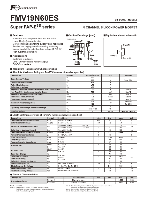
General Description

Drain-Source Voltage Continuous Drain Current Pulsed Drain Current Gate-Source Voltage Repetitive and Non-Repetitive Maximum AvalancheCurrent Non-Repetitive Maximum Avalanche Energy Repetitive Maximum Avalanche Energy Peak Diode Recovery dV/dt Peak Diode Recovery -di/dt Maximum Power Dissipation Operating and Storage Temperature range Isolation Voltage Symbol VDS VDSX ID I DP VGS I AR E AS E AR dV/dt -di/dt PD Tch Tstg VISO Characteristics 600 600 ±19 ±76 ±30 19 799 13 4.8 100 2.16 130 150 -55 to + 150 2 Unit V V A A V A mJ mJ kV/µs A/µs W °C °C kVrms Remarks VGS = -30V Note*1 Note*2 Note*3 Note*4 Note*5 Ta=25°C Tc=25°C t = 60sec, f = 60Hz Electrical Characteristics at Tc=25°C (unless otherwise specified) Description Drain-Source Breakdown Voltage Gate Threshold Voltage Zero Gate Voltage Drain Current Gate-Source Leakage Current Drain-Source On-State Resistance Forward Transconductance Input Capacitance Output Capacitance Reverse Transfer Capacitance Turn-On Time Turn-Off Time Total Gate Charge Gate-Source Charge Gate-Drain Charge Gate-Drain Crossover Charge Avalanche Capability Diode Forward On-Voltage Reverse Recovery Time Reverse Recovery Charge Symbol BVDSS VGS (th) I DSS I GSS R DS (on) gfs Ciss Coss Crss td(on) tr td(off) tf QG Q GS Q GD Q SW I AV VSD trr Qrr Conditions I D =250µA, VGS =0V I D =250µA, VDS =VGS V

Overview

www.DataSheet.co.kr FMV19N60ES Super FAP-E3S series.

Key Features

  • Maintains both low power loss and low noise Lower RDS (on) characteristic More controllable switching dv/dt by gate resistance Smaller VGS ringing waveform during switching Narrow band of the gate threshold voltage (4.2±0.5V) High avalanche durability FUJI POWER MOSFET N-.