BL2303
BL2303 is P-Channel Power Mosfet manufactured by Galaxy Microelectronics.
Production specification
P-Channel Enhancement Mode Field Effect Transistor BL2303
Features
- Electrostatic Sensitive Devices.
- VDS (V) = -30V
- ID = -2.7A(VGS =-10V)
- RDS(ON) < 190mΩ (VGS = -10V)
RDS(ON) < 330mΩ (VGS = -4.5V)
Pb
Lead-free
APPLICATIONS
- P-channel enhancement mode effect transistor.
- Switching application.
ORDERING INFORMATION
Type No.
Marking
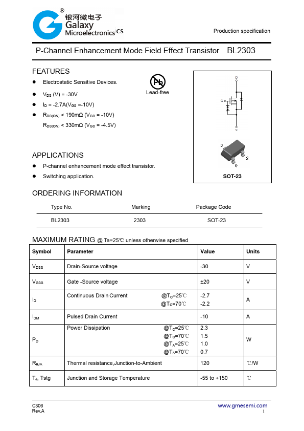
SOT-23
Package Code SOT-23
MAXIMUM RATING @ Ta=25℃ unless otherwise specified
Symbol
Parameter
VDSS
Drain-Source voltage
VGSS ID IDM
RθJA
Gate -Source voltage
Continuous Drain Current
@TC=25℃ @TC=70℃
Pulsed Drain Current
Power...