GI03N70
GI03N70 is N-CHANNEL ENHANCEMENT MODE POWER MOSFET manufactured by GTM.
Description
N-CHANNEL ENHANCEMENT MODE POWER MOSFET
BVDSS RDS(ON) ID
600V 4.0 3.3A
The GI03N70 is specially designed as main switching devices for universal 90~265VAC off-line AC/DC converter applications. The TO-251 package is available for low-profile applications and suited for AC/DC converters.
- Dynamic dv/dt Rating
- Simple Drive Requirement
- Repetitive Avalanche Rated
- Fast Switching Speed
Features
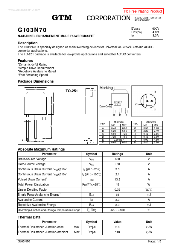
Package Dimensions TO-251
REF. A B C D E F
Millimeter Min. Max. 6.40 6.80 5.20 5.50 6.80 7.20 7.20 7.80 2.30 REF. 0.60 0.90
REF. G H J K L M
Millimeter Min. Max. 0.50 0.70 2.20 2.40 0.45 0.55 0.45 0.60 0.90 1.50 5.40 5.80
Absolute Maximum Ratings
Parameter Drain-Source Voltage Gate-Source Voltage Continuous Drain Current, VGS@10V Continuous Drain Current, VGS@10V Pulsed Drain Current
Symbol VDS VGS ID @TC=25 ID @TC=100 IDM PD @TC=25
Ratings 600 ±30 3.3 2.1 13.2 45 0.36 85 3.3 3.3 -55 ~ +150
Unit V V A A A W W/ m J A m J
Total Power Dissipation Linear Derating Factor Single Pulse Avalanche Energy Avalanche Current Repetitive Avalanche Energy
Operating Junction and Storage Temperature Range
EAS IAR EAR Tj, Tstg
Thermal Data
Parameter Thermal Resistance Junction-case Thermal Resistance Junction-ambient GI03N70 Max. Max. Symbol Rthj-c Rthj-a Value 2.8 110 Unit /W /W Page: 1/5
ISSUED DATE :2005/01/05 REVISED DATE :
Electrical Characteristics (Tj = 25
Parameter Drain-Source Breakdown Voltage
Breakdown Voltage Temperature Coefficient unless otherwise specified)
Min. 600 2.0 Typ. 0.6 2.0 11.4 3.1 4.2 8.4 6 17.7 5.9 600 45 4 p F Max. 4.0 ±1 100 500 4.0 ns n C Unit V V/ V S u A u A u A Test Conditions VGS=0, ID=250u A Reference to 25 , ID=1m A VDS=VGS, ID=250u A VDS=10V, ID=1.6A VGS= ±30V VDS=600V, VGS=0 VDS=480V, VGS=0 VGS=10V, ID=1.6A ID=3.3A VDS=480V VGS=10V VDD=300V ID=3.3A VGS=10V RG=10 RD=91 VGS=0V VDS=25V f=1.0MHz
Symbol BVDSS
BVDSS / Tj
Gate Threshold Voltage Forward Transconductance Gate-Source Leakage Current
Drain-Source Leakage Current(Tj=25 )...