• Part: 2SK3069
  • Description: N-Channel MOSFET
  • Category: MOSFET
  • Manufacturer: Hitachi Semiconductor
  • Size: 52.09 KB
Download 2SK3069 Datasheet PDF
Hitachi Semiconductor
2SK3069
2SK3069 is N-Channel MOSFET manufactured by Hitachi Semiconductor.
Features - Low on-resistance R DS(on) = 6 mΩ typ. - Low drive current - 
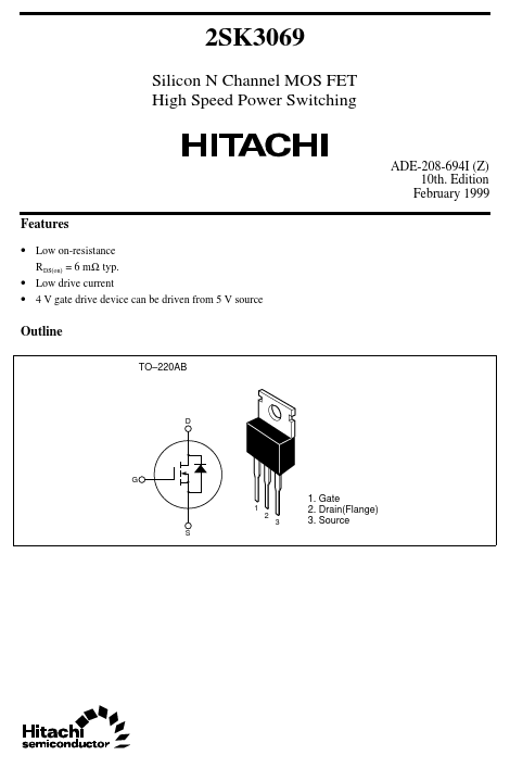
4 V gate drive device can be driven from 5 V source Outline TO- 220AB 1 2 S 3 1. Gate 2. Drain(Flange) 3. Source Absolute Maximum Ratings (Ta = 25°C) Item Drain to source voltage Gate to source voltage Drain current Drain peak current Body-drain diode reverse drain current Avalanche current Avalanche energy Channel dissipation Channel temperature Storage temperature Note: Symbol VDSS VGSS ID I D(pulse) I DR I AP Note 3 Note 3 Note 2 Note 1 Ratings 60 ±20 75 300 75 50 214 100 150 - 55 to +150 Unit V V A A A A m J W °C °C EAR Pch Tch Tstg 1. PW ≤ 10 µs, duty cycle ≤ 1% 2. Value at Tc = 25°C 3. Value at Tch = 25°C, Rg ≥ 50 Ω Electrical Characteristics (Ta = 25°C) Item Symbol Min 60 - - 1.0 - - |yfs| Ciss Coss Crss Qg Qgs Qgd t d(on) tr t d(off) tf VDF t rr 50 - - - - - - - - - - - - Typ - - - - 6.0 8.0 80 7100 1000 280 125 25 25 60 300 520 330 1.05 90 Max - ±0.1 10 2.5 7.5 12 - - - - - - - - - - - - - Unit V µA µA V mΩ mΩ S p F p F p F nc nc nc ns ns ns ns V ns I F = 75 A, VGS = 0 I F = 75 A, VGS = 0 di F/ dt = 50 A/ µs Test Conditions I D = 10 m A, VGS = 0 VGS = ±20 V, VDS = 0 VDS = 60 V, VGS = 0 I D = 1 m A, VDS = 10 V Note 1 I D = 40 A, VGS = 10 V Note 1 I D = 40 A, VGS = 4 V Note 1 I D = 40 A, VDS = 10 V Note 1 VDS = 10 V VGS = 0 f = 1 MHz VDD = 25 V VGS = 10 V I D = 75 A VGS = 10 V, ID = 40 A RL = 0.75 Ω Drain to source breakdown voltage V(BR)DSS Gate to source leak current Zero gate voltege drain current Gate to source cutoff voltage Static drain to source on state resistance Forward transfer admittance Input capacitance Output capacitance Reverse transfer capacitance Total gate charge Gate to source charge Gate to drain charge Turn-on delay time Rise time Turn-off delay time Fall time Body- drain diode forward voltage Body- drain diode reverse recovery time Note: 1. Pulse test I GSS I DSS VGS(off) RDS(on) Main Characteristics...