3SK194
3SK194 is Silicon N-Channel Dual Gate MOS FET manufactured by Hitachi Semiconductor.
Silicon N-Channel Dual Gate MOS FET
Application
VHF/UHF TV tuner RF amplifier
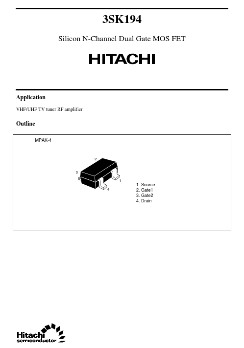
Outline
MPAK-4
3 1 4
1. Source 2. Gate1 3. Gate2 4. Drain
Absolute Maximum Ratings (Ta = 25°C)
Item Drain to source voltage Gate 1 to source voltage Gate 2 to source voltage Drain current Channel power dissipation Channel temperature Storage temperature Symbol VDS VG1S VG2S ID Pch Tch Tstg Ratings 15 ±10 ±10 35 150 125
- 55 to +125 Unit V V V m A m W °C °C
Electrical Characteristics (Ta = 25°C)
Item Drain to source breakdown voltage Gate 1 to source breakdown voltage Gate 2 to source breakdown voltage Gate 1 cutoff current Gate 2 cutoff current Symbol V(BR)DSX V(BR)G1SS V(BR)G2SS I G1SS I G2SS Min 15 ±10 ±10
- -
- - 0 17
- -
- 12
- - 27
- Typ
- -
- -
- -
- -
- 2.8 1.8 0.02 15 3.0 3.0 30 1.0 Max
- -
- ±100 ±100
- 1.0
- 1.5 10
- 3.5 2.5
- - 4.5 4.0
- 2.5 Unit V V V n A n A V V m A m S p F p F p F d B d B d B d B d B VDD = 12 V, VAGC = 10.5 V, f = 60 MHz VDS = 6 V, VG2S = 3 V, I D = 10 m A, f = 200 MHz VDS = 6 V, VG2S = 3 V, I D = 10 m A, f = 900 MHz Test conditions I D = 200 µA, VG1S = VG2S =
- 5 V I G1 = ±10 µA, VG2S = VDS = 0 I G2 = ±10 µA, VG1S = VDS = 0 VG1S = ±8 V, V G2S = VDS = 0 VG2S = ±8 V, V G1S = VDS = 0 VDS = 10 V, VG2S = 3 V, I D = 100 µA VDS = 10 V, VG1S = 3 V, I D = 100 µA VDS = 6 V, VG1S = 0, VG2S = 3 V VDS = 6 V, VG2S = 3 V, I D = 10 m A, f = 1 k Hz VDS = 6 V, VG2S = 3 V, I D = 10 m A, f = 1 MHz
Gate 1 to source cutoff voltage VG1S(off) Gate 2 to source cutoff voltage VG2S(off) Drain current Forward transfer admittance Input capacitance Output capacitance Reverse transfer capacitance Power gain Noise figure Noise figure Power gain Noise figure Note: Marking is “IY- ”. I DSS |yfs| Ciss Coss Crss PG NF NF PG NF
Maximum Channel Power Dissipation Curve Channel Power Dissipation Pch (m W) 300 20 0.8 0.6 Drain Current ID (m A) 16 0.4 Typical Output Characteristics VG2S = 3 V
0.2 VG1S =...