Datasheet Summary
..
HY5DU12422A(L)T HY5DU12822A(L)T HY5DU121622A(L)T
512Mb DDR SDRAM
HY5DU12422A(L)T HY5DU12822A(L)T HY5DU121622A(L)T
This document is a general product description and is subject to change without notice. Hynix semiconductor does not assume any responsibility for use of circuits described. No patent licenses are implied. Rev. 0.0/Feb. 2003 1
..
HY5DU12422A(L)T HY5DU12822A(L)T HY5DU121622A(L)T
Revision History
1. Rev 0.0 (Feb. 19)
1) Datasheet Release in Preliminary version
Rev. 0.0/Feb. 2003
..
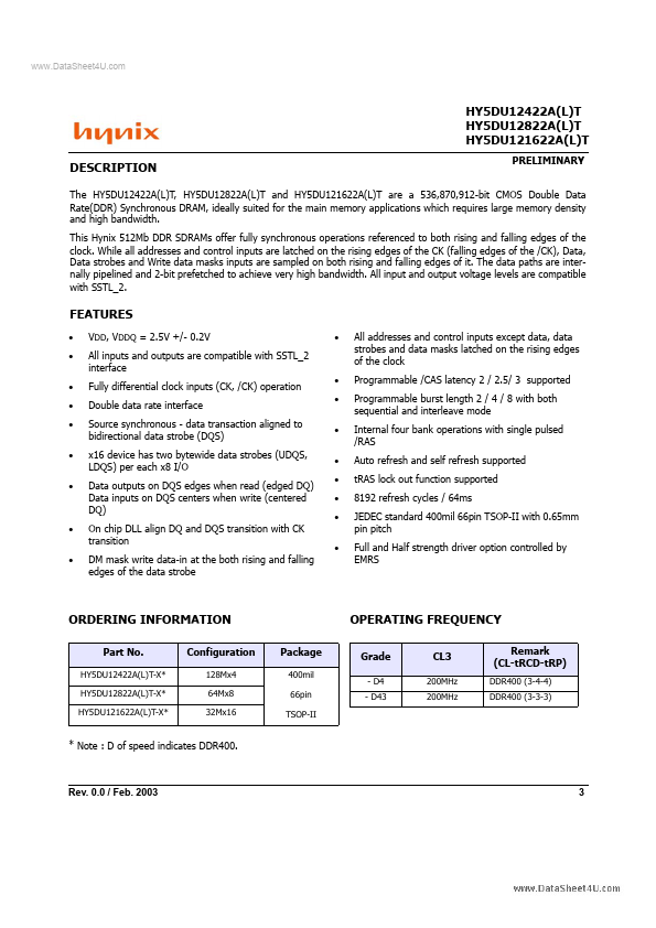
HY5DU12422A(L)T HY5DU12822A(L)T HY5DU121622A(L)T DESCRIPTION
PRELIMINARY
The HY5DU12422A(L)T, HY5DU12822A(L)T and HY5DU121622A(L)T are...


