Datasheet Summary
512Mb(32Mx16) GDDR SDRAM
This document is a general product description and is subject to change without notice. Hynix Semiconductor does not assume any responsibility for use of circuits described. No patent licenses are implied. Rev. 0.3 / Apr. 2005 1
1HY5DU121622CTP
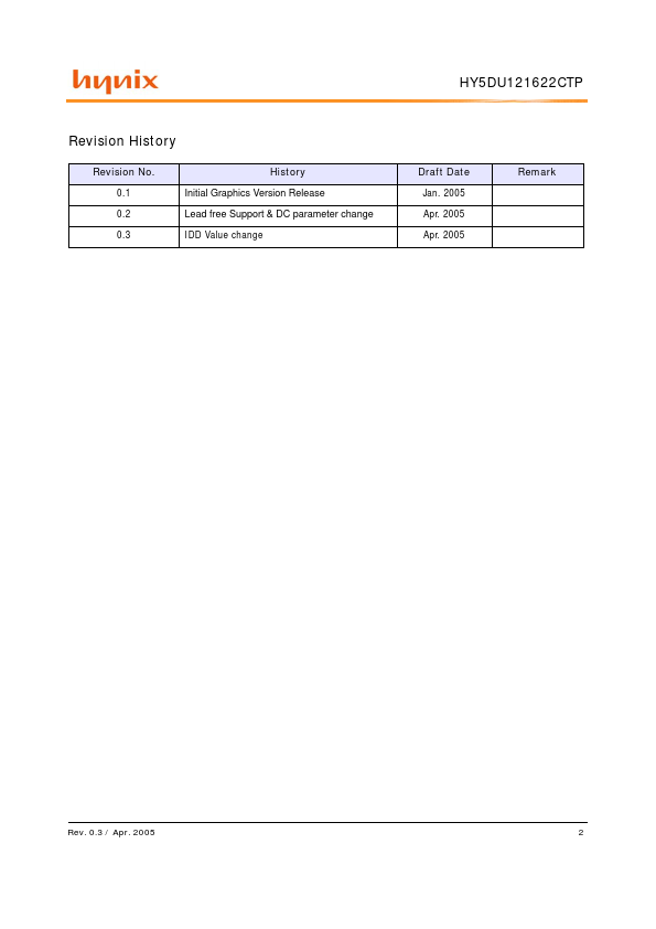
Revision History
Revision No. 0.1 0.2 0.3 History Initial Graphics Version Release Lead free Support & DC parameter change IDD Value change Draft Date Jan. 2005 Apr. 2005 Apr. 2005 Remark
Rev. 0.3 / Apr. 2005
1HY5DU121622CTP
Preliminary
DESCRIPTION
The HY5DU121622CTP is a 536,870,912-bit CMOS Double Data Rate(DDR) Synchronous DRAM, ideally suited for the main memory applications which...