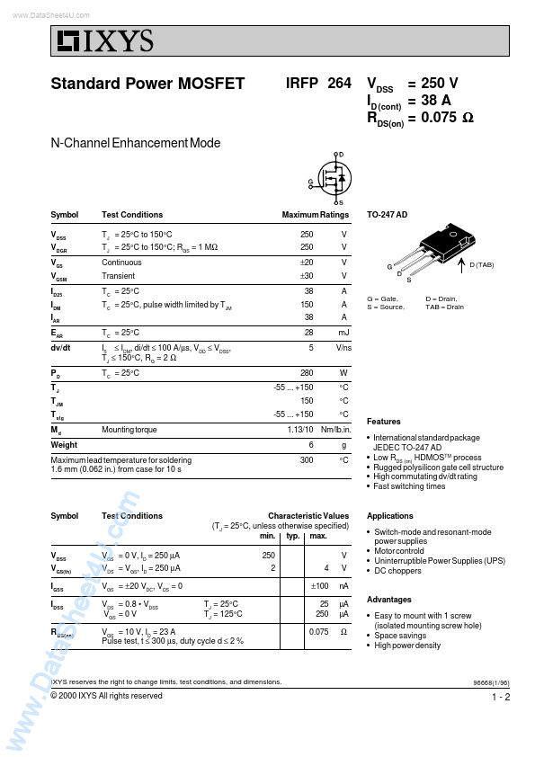
13/10 Nm/. 6 300 g °C l l l l Maximum lead temperature for soldering 1.6 mm (0.062 in.) from case for 10 s International standard package JEDEC TO-247 AD Low RDS (on) HDMOSTM process Rugged polysilicon gate cell structure High commutating dv/dt rating Fast switching times ww w.D ata Sh eet 4U .co m Symbol Test Conditions Characteristic Values (TJ = 25°C, unless otherwise specified) min. typ. max. 250 2 4 ±100 TJ = 25°C TJ = 125°C 25 250 0.075 V V nA µA µA Ω