IXFK120N25P Description
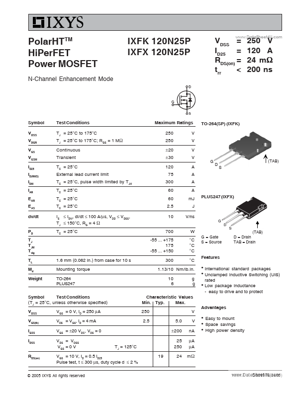
PolarHTTM HiPerFET Power MOSFET N-Channel Enhancement Mode IXFK 120N25P IXFX 120N25P VDSS = ID25 = RDS(on) = trr < .. 250 V 120 A 24 mΩ 200 ns Symbol VDSS VDGR VGS VGSM ID25 ID(RMS) IDM IAR EAR EAS dv/dt PD TJ TJM Tstg TL Md Weight Test Conditions TJ = 25°C to 175°C TJ = 25°C to 175°C; +150 V V V V TO-264(SP) (IXFK) G A A A A mJ J V/ns W °C °C °C °C D (TAB) S PLUS247 (IXFX) G = Gate S = Source (TAB) D = Drain TAB =...
IXFK120N25P Key Features
- easy to drive and to protect
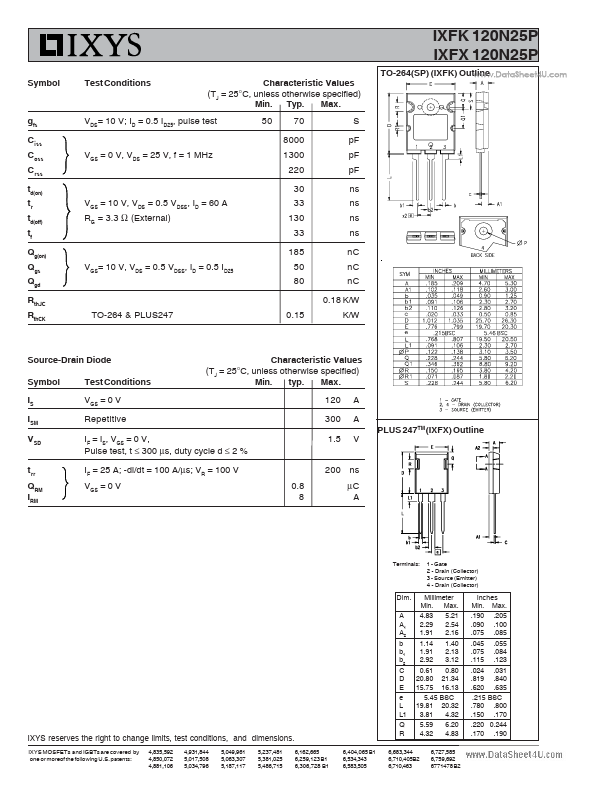
- Gate 2
- Drain (Collector) 3
- Source (Emitter) 4
- Drain (Collector)