MJD2955 Overview
Description
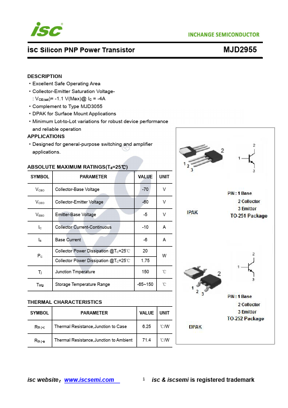
Excellent Safe Operating Area - Collector-Emitter Saturation Voltage- : VCE(sat)= -1.1 V(Max)@ IC = -4A - Complement to Type MJD3055 - DPAK for Surface Mount Applications - Minimum Lot-to-Lot variations for robust device performance and reliable operation APPLICATIONS - Designed for general-purpose switching and amplifier.