BSB024N03LXG
BSB024N03LXG is Power MOSFET manufactured by Infineon.
Features
- Pb-free plating; Ro HS pliant
- Dual sided cooling
- Low profile (<0.7 mm)
- 100% avalanche tested
- Qualified for consumer level application
- Excellent gate charge x R DS(on) product (FOM)
- Very low on-resistance R DS(on)
- Optimized for high switching frequency DC/DC converter
- Low parasitic inductance
Product Summary V DS R DS(on),max ID 30 2.4 145 V mΩ A
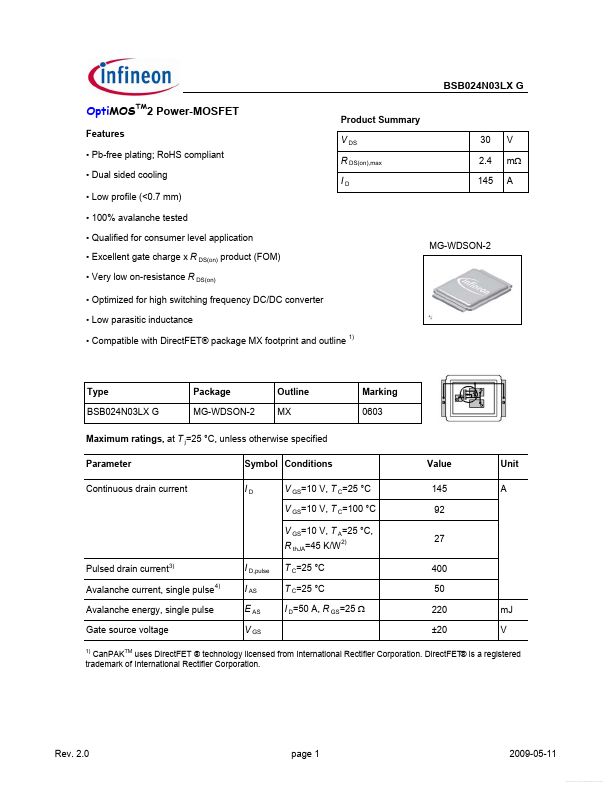
MG-WDSON-2
- patible with Direct FET® package MX footprint and outline 1)
Type BSB024N03LX G
Package MG-WDSON-2
Outline MX
Marking 0603
Maximum ratings, at T j=25 °C, unless otherwise specified Parameter Continuous drain current Symbol Conditions ID V GS=10 V, T C=25 °C V GS=10 V, T C=100 °C V GS=10 V, T A=25 °C, R th JA=45 K/W 2) Pulsed drain current3) Avalanche current, single pulse 4) Avalanche energy, single pulse Gate source voltage I D,pulse I AS E AS V GS T C=25 °C T C=25 °C I D=50 A, R GS=25 Ω Value 145 92 27 400 50 220 ±20 m J V Unit A
1) Can PAKTM uses Direct FET ® technology licensed from International Rectifier Corporation. Direct FET® is a registered trademark of International Rectifier Corporation.
Rev. 2.0 page 1
2009-05-11
Free Datasheet http://../
BSB024N03LX G
Maximum ratings, at T j=25 °C, unless otherwise specified Parameter Power dissipation Symbol Conditions P tot T C=25 °C T A=25 °C, R th JA=45 K/W 2) Operating and storage temperature IEC climatic category; DIN IEC 68-1 T j, T stg Value 78 2.8 -40 ... 150 55/150/56 °C Unit W
Parameter
Symbol Conditions min.
Values typ. max.
Unit
Thermal characteristics Thermal resistance, junction
- case R th JC bottom top Device on PCB R th JA 6 cm2 cooling area2) 1.0 1.6 45 K/W
Electrical characteristics, at T j=25 °C, unless otherwise specified Static characteristics Drain-source breakdown voltage Gate threshold voltage Zero gate voltage drain current V (BR)DSS V GS=0 V, I D=1 m A V GS(th) I DSS V DS=V GS, I D=250 µA V DS=30 V, V GS=0 V, T j=25 °C V DS=30 V, V GS=0 V, T j=125 °C Gate-source leakage current Drain-source on-state...