Datasheet4U Logo Datasheet4U.com

ICSSSTUF32864A - 25-Bit Configurable Registered Buffer for DDR2

Datasheet Summary

Description

This 25-bit 1:1 or 14-bit 1:2 configurable registered buffer is designed for 1.7-V to 1.9-V VDD operation.

All clock and data inputs are compatible with the JEDEC standard for SSTL_18.

The control inputs are LVCMOS.

Features

  • 25-bit 1:1 or 14-bit 1:2 configurable registered buffer.
  • Supports SSTL_18 JEDEC specification on data inputs and outputs.
  • Supports LVCMOS switching levels on C0, C1 and RESET# inputs.
  • Low voltage operation VDD = 1.7V to 1.9V.
  • Available in 96 BGA package.
  • Drop-in replacement for ICSSSTUF32866.
  • Green packages available
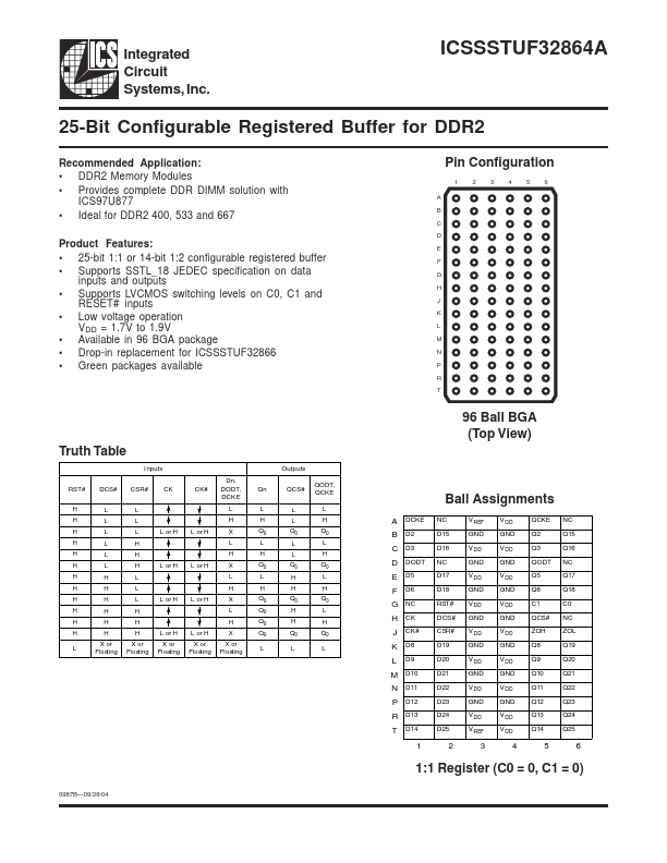
 Pin Configuration 1 A B C D E F G H J K L M N P R T 2 3 4 5 6 96 Ball BGA (Top View) Truth Table I nputs RST# H H.

📥 Download Datasheet

Datasheet preview – ICSSSTUF32864A

Datasheet Details

Part number ICSSSTUF32864A
Manufacturer Integrated Circuit Systems
File Size 111.62 KB
Description 25-Bit Configurable Registered Buffer for DDR2
Datasheet download datasheet ICSSSTUF32864A Datasheet
Additional preview pages of the ICSSSTUF32864A datasheet.
Other Datasheets by Integrated Circuit Systems

Full PDF Text Transcription

Click to expand full text
Integrated Circuit Systems, Inc. ICSSSTUF32864A 25-Bit Configurable Registered Buffer for DDR2 Recommended Application: • DDR2 Memory Modules • Provides complete DDR DIMM solution with ICS97U877 • Ideal for DDR2 400, 533 and 667 Product Features: • 25-bit 1:1 or 14-bit 1:2 configurable registered buffer • Supports SSTL_18 JEDEC specification on data inputs and outputs • Supports LVCMOS switching levels on C0, C1 and RESET# inputs • Low voltage operation VDD = 1.7V to 1.
Published: |