IS45S16400C1
IS45S16400C1 is 1 Meg Bits x 16 Bits x 4 Banks (64-MBIT) SYNCHRONOUS DYNAMIC RAM manufactured by ISSI.
FEATURES
- Clock frequency: 143 MHz
- Fully synchronous; all signals referenced to a positive clock edge
- Internal bank for hiding row access/precharge
- Single 3.3V power supply
- LVTTL interface
- Programmable burst length
- (1, 2, 4, 8, full page)
- Programmable burst sequence: Sequential/Interleave
- Self refresh modes
- 4096 refresh cycles every 64 ms
- Random column address every clock cycle
- Programmable CAS latency (2, 3 clocks)
- Burst read/write and burst read/single write operations capability
- Burst termination by burst stop and precharge mand
- Byte controlled by LDQM and UDQM
- Automotive Temperature Range Option A: 0o C to +70o C Option A1: -40o C to +85o C
- Package: 400-mil 54-pin TSOP II
- Lead-free package is available
..
ISSI
®
OCTOBER 2005
OVERVIEW
ISSI's 64Mb Synchronous DRAM IS45S16400C1 is organized as 1,048,576 bits x 16-bit x 4-bank for improved performance. The synchronous DRAMs achieve high-speed data transfer using pipeline architecture. All inputs and outputs signals refer to the rising edge of the clock input.
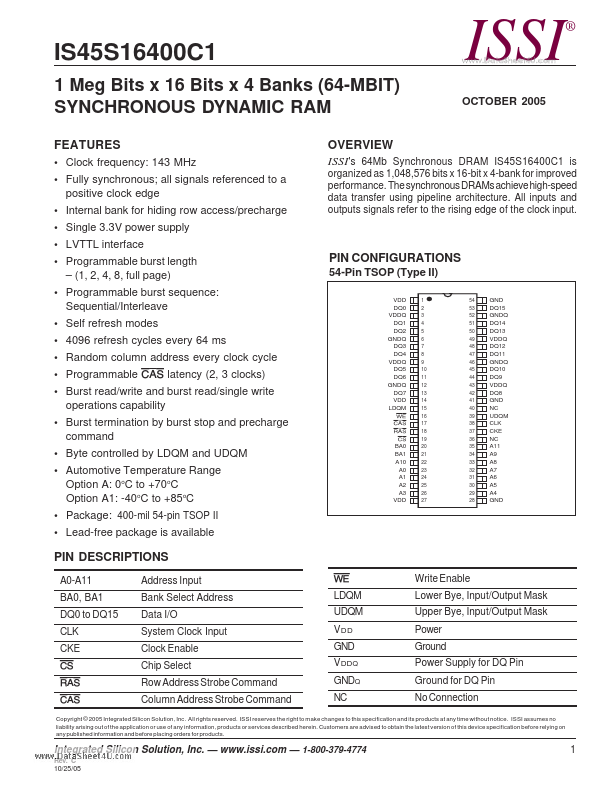
PIN CONFIGURATIONS
54-Pin TSOP (Type II)
VDD DQ0 VDDQ DQ1 DQ2 GNDQ DQ3 DQ4 VDDQ DQ5 DQ6 GNDQ DQ7 VDD LDQM WE CAS RAS CS BA0 BA1 A10 A0 A1 A2 A3 VDD 1 2 3 4 5 6 7 8 9 10 11 12 13 14 15 16 17 18 19 20 21 22 23 24 25 26 27 54 53 52 51 50 49 48 47 46 45 44 43 42 41 40 39 38 37 36 35 34 33 32 31 30 29 28 GND DQ15 GNDQ DQ14 DQ13 VDDQ DQ12 DQ11 GNDQ DQ10 DQ9 VDDQ DQ8 GND NC UDQM CLK CKE NC A11 A9 A8 A7 A6 A5 A4 GND
PIN DESCRIPTIONS
A0-A11 BA0, BA1 DQ0 to DQ15 CLK CKE CS RAS CAS Address Input Bank Select Address Data I/O System Clock Input Clock Enable Chip Select Row Address Strobe mand Column Address Strobe mand WE LDQM UDQM VDD GND VDDQ GNDQ NC Write Enable Lower Bye, Input/Output Mask Upper Bye, Input/Output Mask Power Ground Power Supply for DQ Pin Ground for DQ Pin No Connection
Copyright © 2005 Integrated Silicon Solution, Inc. All rights reserved. ISSI reserves the right to make changes to this specification and its...


