Datasheet4U Logo Datasheet4U.com

IRF6616PBF - Power MOSFET

General Description

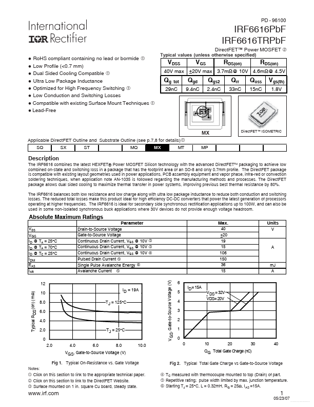
The IRF6616 combines the latest HEXFET® Power MOSFET Silicon technology with the advanced DirectFETTM packaging to achieve low combined on-state and switching loss in a package that has the footprint area of an SO-8 and only 0.7mm profile.

Key Features

  • e Pulse 0 1 10 100 1000 1.00 1 0.10 VGS = 0V 0.0 0.1 0.2 0.3 0.4 0.5 0.6 0.7 0.8 0.9 1.0 1.1 VSD, Source-to-Drain Voltage (V) 0.1 VDS , Drain-to-Source Voltage (V) Fig 10. Typical Source-Drain Diode Forward Voltage 120 100 ID, Drain Current (A) Typical VGS(th) Gate threshold Voltage (V) 2.5 Fig11. Maximum Safe Operating Area 80 60 40 20 0 25 50 75 100 125 150 T C , Case Temperature (°C) 2.0 ID = 250µA 1.5 1.0 -75 -50 -25 0 25 50 75 100 125 150 T J , Junction Temperature ( °C ) Fig.

📥 Download Datasheet

Full PDF Text Transcription (Reference)

The following content is an automatically extracted verbatim text from the original manufacturer datasheet and is provided for reference purposes only.

View original datasheet text
IRF6616PbF IRF6616TRPbF RoHS compliant containing no lead or bormide  l Low Profile (<0.7 mm) l Dual Sided Cooling Compatible  l Ultra Low Package Inductance l Optimized for High Frequency Switching  l Low Conduction and Switching Losses l Compatible with existing Surface Mount Techniques  l Lead-Free l PD - 96100 Typical values (unless otherwise specified) DirectFET™ Power MOSFET ‚ VDSS VGS RDS(on) RDS(on) 40V max ±20V max 3.7mΩ@ 10V 4.6mΩ@ 4.5V Qg tot Qgd 9.4nC Qgs2 2.4nC Qrr 33nC Qoss 15nC Vgs(th) 1.8V 29nC MX Applicable DirectFET Outline and Substrate Outline (see p.