IRF6691TRPBF
IRF6691TRPBF is Power MOSFET manufactured by International Rectifier.
- Part of the IRF6691PBF comparator family.
- Part of the IRF6691PBF comparator family.
Description
The IRF6691Pb F bines the latest HEXFET® Power MOSFET Silicon technology with the advanced Direct FETTM packaging to achieve the lowest on-state resistance in a package that has the footprint of a SO-8 and only 0.7 mm profile. The Direct FET package is patible with existing layout geometries used in power applications, PCB assembly equipment and vapor phase, infra-red or convection soldering techniques. Application note AN-1035 is followed regarding the manufacturing methods and processes. The Direct FET package allows dual sided cooling to maximize thermal transfer in power systems, improving previous best thermal resistance by 80%. The IRF6691Pb F balances industry leading on-state resistance while minimizing gate charge along with ultra low package inductance to reduce both conduction and switching losses. This part contains an integrated Schottky diode to reduce the Qrr of the body drain diode further reducing the losses in a Synchronous Buck circuit. The reduced losses make this product ideal for high frequency/high efficiency DC-DC converters that power high current loads such as the latest generation of microprocessors. The IRF6691Pb F has been optimized for parameters that are critical in synchronous buck converter’s Sync FET sockets.
Absolute Maximum Ratings
Parameter
VDS VGS ID @ TA = 25°C ID @ TA = 70°C ID @ TC = 25°C IDM EAS IAR
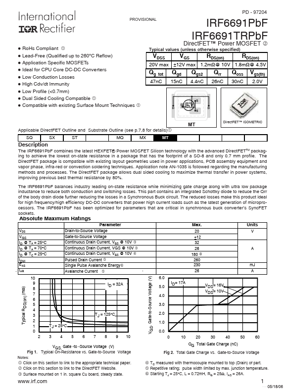
10 9 8 7 6 5 4 3 2 1 0 2
Max.
Units
Drain-to-Source Voltage Gate-to-Source Voltage Continuous Drain Current, VGS @ 10V
Continuous Drain Current, VGS @ 10V Continuous Drain Current, VGS @ 10V Pulsed Drain Current Single Pulse Avalanche Energy Avalanche Current g e e f
Ãg h
VGS, Gate-to-Source Voltage (V)
20 ±12 32 26 180 260 230 26
6.0 5.0 4.0 3.0 2.0 1.0 0.0 0 10 20 ID= 17A j
A m J A
VDS= 16V VDS= 10V
Typical RDS(on) (mΩ)
ID = 32A
T J = 125°C T J = 25°C 3 4 5 6 7 8 9 10
VGS, Gate -to -Source Voltage (V) Fig 1. Typical On-Resistance vs. Gate-to-Source Voltage Notes: Click on this section...