will impact the MOSFETs’ susceptibility to Cdv/dt turn on. The drain of Q2 is connected to the switching node of the converter and therefore sees transitions between ground and Vin. As Q1 turns on and off there is a rate of change of drain voltage dV/dt which is capacitively coupled to the gate of Q2 and can induce a voltage spike on the gate that is sufficient to turn the MOSFET on, resulting in shoot-through current . The ratio of Qgd/Qgs1 must be minimized to reduce the potential for Cdv/dt t.
Full PDF Text Transcription for IRF7475PBF (Reference)
Note: Below is a high-fidelity text extraction (approx. 800 characters) for
IRF7475PBF. For precise diagrams, and layout, please refer to the original PDF.
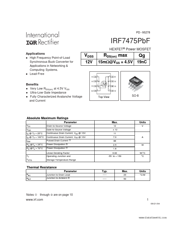
PD - 95278 IRF7475PbF HEXFET® Power MOSFET Applications l High Frequency Point-of-Load Synchronous Buck Converter for Applications in Networking & Computing Systems. l Le...
View more extracted text
uck Converter for Applications in Networking & Computing Systems. l Lead-Free Benefits l Very Low RDS(on) at 4.5V VGS l Ultra-Low Gate Impedance l Fully Characterized Avalanche Voltage and Current VDSS 12V 15m:@VGS = 4.5V 1 8 7 RDS(on) max Qg 19nC S S S G A A D D D D 2 3 6 4 5 Top View SO-8 Absolute Maximum Ratings Parameter VDS VGS ID @ TA = 25°C ID @ TA = 100°C IDM PD @TA = 25°C PD @TA = 70°C TJ TSTG Drain-to-Source Voltage Gate-to-Source Voltage Continuous Drain Current, VGS @ 10V Continuous Drain Current, VGS @ 10V Pulsed Drain Current Max. 12 ± 12 11 7.0 88 2.5 1.6 0.
More Datasheets from International Rectifier (now Infineon)