JCST 2N7002K
N-channel MOSFET
| Part No. | 2N7002K |
|---|---|
| Datasheet | 2N7002K Download |
| Manufacturer |  JCST |
| Description | N-channel MOSFET |
| Buy | Stock & Price |
FEATURES
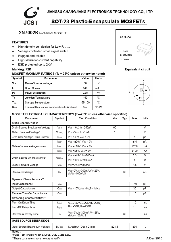
z High density cell design for Low RDS(on) z Voltage controlled small signal switch z Rugged and reliable z High saturation current capability z ESD protected up to 2KV Marking: 72K MOSFETMAXIMUM RATINGS
(Ta = 25°C unless otherwise noted) Symbol Parameter Value Units VDS Drain-Source voltage 60 V ID Drain Current 340 mA PD Power Dissipation 0.35 W TJ Junction Temperature 150 ℃ Tstg Storage Temperature -55-150 ℃ RθJA Thermal Resistance fromJunction to Ambient 357 ℃ /W SOT-23 1. GATE 2. SOURCE 3. DRAIN Equivalent circuit MOSFETELECTRICAL CHARACTERISTICS
(Ta=25℃ unless otherwise specified) Parameter Symbol Test Condition Min Typ Static Characteristics Drain-Source Breakdown Voltage VDS VGS = 0V, ID =250µA 60 Gate Threshold Voltage* VGS(th) VDS =VGS, ID =1mA 1 Zero Gate Voltage Drain Current IDSS VDS =48V,VGS = 0V IGSS1 VGS =±20V, VDS = 0V Gate –Source leakage current IGSS2 VGS =±10V, VDS = 0V IGSS3 VGS =±5V, VDS = 0V Drain-Source On-Resistance* RDS(on) VGS = 4.5V, ID =200mA VGS =10V,ID =500mA Diode Forward Voltage VSD VGS=0V, IS=300mA Recovered charge Qr VGS=0V,IS=300mA,VR=25V, dls/dt=-100A/µS 30 Max Units 1 ±10 ±200 ±100 5.