2N7002KU
Key Features
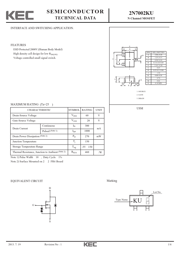
- DRAIN USM EQUIVALENT CIRCUIT D G S Marking KUType Name Lot No
| Part Number | Manufacturer | Description |
|---|---|---|
| 2N7002KU | Kodenshi AUK Group | N-channel MOSFET |
| 2N7002K | LITEON | N-channel MOSFET |
| 2N7002KT | Micro Commercial Components | N-Channel MOSFET |
| 2N7002K2 | Silikron | MOSFET |
| 2N7002X | JCET | N-Channel MOSFET |
| 2N7002-G | Supertex | N-Channel Enhancement-Mode Vertical DMOS FETs |
| 2N7002 | Nexperia | 300mA N-channel MOSFET |
| 2N7002SWLT1 | WILLAS | N-Channel Small Signal MOSFET |
| 2N7002 | Diodes Incorporated | N-CHANNEL ENHANCEMENT MODE FIELD EFFECT TRANSISTOR |
| 2N7002Q | Diodes Incorporated | N-CHANNEL ENHANCEMENT MODE FIELD EFFECT TRANSISTOR |