2N7002X
Description
JIANGSU CHANGJIANG ELECTRONICS TECHNOLOGY CO., LTD SOT-89-3L Plastic-Encap sulate MOSFETS 2N7002X V(BR)DSS 60 V MOSFET( N-Channel ) RDS(on)MAX 5Ω@10V 7Ω@5V ID 115mA SOT-89-3L 2. DRAIN 3. SOURCE ...
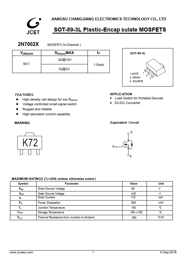
JIANGSU CHANGJIANG ELECTRONICS TECHNOLOGY CO., LTD SOT-89-3L Plastic-Encap sulate MOSFETS 2N7002X V(BR)DSS 60 V MOSFET( N-Channel ) RDS(on)MAX 5Ω@10V 7Ω@5V ID 115mA SOT-89-3L 2. DRAIN 3. SOURCE ...
| Part Number | Manufacturer | Description |
|---|---|---|
| 2N7002DWA | Diodes Incorporated | DUAL N-CHANNEL MOSFET |
| 2N7002K | JCST | N-channel MOSFET |
| 2N7002H | Diodes Incorporated | N-Channel MOSFET |
| 2N7002ZDW | Unisonic Technologies | DUAL N-CHANNEL POWER MOSFET |
| 2N7002K | LITEON | N-channel MOSFET |
| 2N7002K | Rectron | N-Channel Enhancement Mode Power MOSFET |
| 2N7002KA | Micro Commercial Components | N-Channel MOSFET |
| 2N7002DWS | Diodes Incorporated | DUAL N-CHANNEL MOSFET |
| 2N7002 | Diodes Incorporated | N-CHANNEL ENHANCEMENT MODE FIELD EFFECT TRANSISTOR |
| 2N7002 | Kexin Semiconductor | N-Channel Enhancement MOSFET |