SI9926
SI9926 is Dual N-Channel MOSFET manufactured by Kexin Semiconductor.
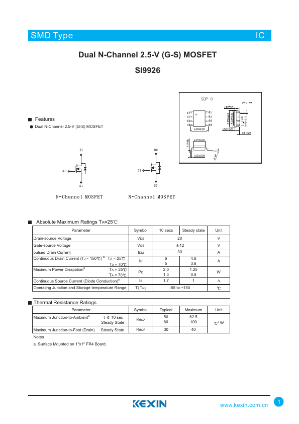
Features
Dual N-Channel 2.5-V (G-S) MOSFET
Absolute Maximum Ratings TA=25
Parameter
Drain-source Voltage
Gate-source Voltage pulsed Drain Current
Continuous Drain Current (TJ = 150 ) a TA = 25
Maximum Power Disspationa
TA = 70 TA = 25
TA = 70 Continuous Source Current (Diode Conduction)a
Operating Junction and Storage temperature Range
Symbol VDS VGS IDM ID
PD IS Tj Tstg
10 secs Steady state
12 30 6 4.8 5 3.8 2.0 1.25 1.3 0.8 1.7 1 -55 to +150
Unit V V A A
Thermal Resistance Ratings
Parameter
Maximum Junction-to-Ambienta t 10 sec Steady State
Maximum Junction-to-Foot (Drain) Steady State
Notes a. Surface Mounted on 1''x1'' FR4 Board.
Symbol Rth JA Rth JF
Typical
50 80
Maximum
62.5 100
Unit /W
.kexin..cn 1
SMD Type
Electrical Characteristics TA=25
Parameter Gate Threshold Voltage Gate-Body Leakage Current, Reverse
Zero Gate Voltage Drain Current
On-State Drain Current- 1
Static Drain-Source On-State Resistance
-...