2SD1614
Features
- High DC Current Gain:h FE 135 to 600.
- Low VCE(sat)
- plementary to 2SB1114
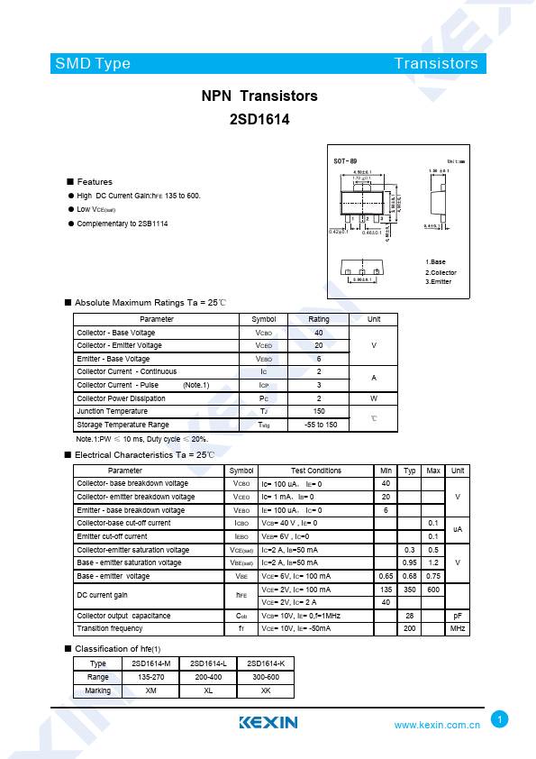
1.70 0.1
0.42 0.1
0.46 0.1
- Absolute Maximum Ratings Ta = 25℃
Parameter
Collector
- Base Voltage
Collector
- Emitter Voltage Emitter
- Base Voltage
Collector Current
- Continuous
Collector Current
- Pulse
(Note.1)
Collector Power Dissipation
Junction Temperature
Storage Temperature Range
Note.1:PW ≤ 10 ms, Duty cycle ≤ 20%.
- Electrical Characteristics Ta = 25℃
Symbol VCBO VCEO VEBO IC ICP PC TJ Tstg
Rating 40 20 6 2 3 2 150
-55 to 150
Parameter Collector- base breakdown voltage Collector- emitter breakdown voltage Emitter
- base breakdown voltage Collector-base cut-off current Emitter cut-off current Collector-emitter saturation voltage Base
- emitter saturation voltage Base
- emitter voltage
DC current gain
Collector output capacitance Transition frequency
Symbol
Test Conditions
VCBO Ic= 100 u A, IE= 0
VCEO Ic= 1 m A,IB= 0
VEBO IE= 100 u A, IC= 0
ICBO VCB= 40 V , IE= 0
IEBO...