2SD1619
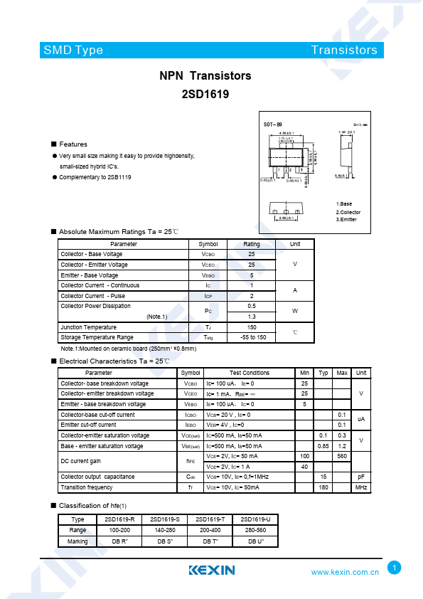
Features
- Very small size making it easy to provide highdensity, small-sized hybrid IC’s.
- plementary to 2SB1119
1.70 0.1
0.42 0.1
0.46 0.1
- Absolute Maximum Ratings Ta = 25℃
Parameter
Symbol
Collector
- Base Voltage
VCBO
Collector
- Emitter Voltage
VCEO
Emitter
- Base Voltage
VEBO
Collector Current
- Continuous
Collector Current
- Pulse
Collector Power Dissipation PC
(Note.1)
Junction Temperature
Storage Temperature Range
Tstg
Note.1:Mounted on ceramic board (250mm2 ×0.8mm)
Rating 25 25 5 1 2 0.5 1.3 150
-55 to 150
- Electrical Characteristics Ta = 25℃
Parameter Collector- base breakdown voltage Collector- emitter breakdown voltage Emitter
- base breakdown voltage Collector-base cut-off current Emitter cut-off current Collector-emitter saturation voltage Base
- emitter saturation voltage
DC current gain
Collector output capacitance Transition frequency
Symbol...