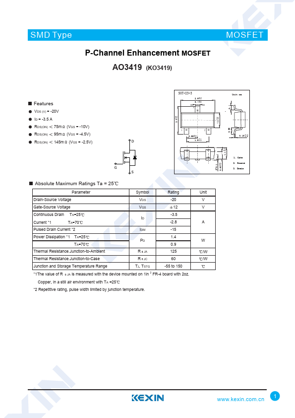
AO3419 Overview
Key Specifications
Package: TO-236-3
Mount Type: Surface Mount
Pins: 3
Height: 1.25 mm
| Part | AO3419 |
|---|---|
| Description | P-Channel Enhancement MOSFET |
| Category | MOSFET |
| Manufacturer | Kexin Semiconductor |
| Size | 1.23 MB |
Package: TO-236-3
Mount Type: Surface Mount
Pins: 3
Height: 1.25 mm
| Seller | Inventory | Price Breaks | Buy |
|---|---|---|---|
| DigiKey | 102145 | 1+ : 0.49 USD 10+ : 0.298 USD 100+ : 0.1886 USD 500+ : 0.14102 USD |
View Offer |
| DigiKey | 102145 | 1+ : 0.49 USD 10+ : 0.298 USD 100+ : 0.1886 USD 500+ : 0.14102 USD |
View Offer |
| Part Number | Manufacturer | Description |
|---|---|---|
| AO3419 | Alpha & Omega Semiconductors | 20V P-Channel MOSFET |
| AO3413 | Alpha & Omega Semiconductors | 20V P-Channel MOSFET |
| AO3415 | Alpha & Omega Semiconductors | 20V P-Channel MOSFET |
| AO3416 | Alpha & Omega Semiconductors | 20V N-Channel MOSFET |
| AO3414L | Alpha & Omega Semiconductors | N-Channel MOSFET |