Datasheet4U Logo Datasheet4U.com

KPA1873 - MOS Field Effect Transistor

Datasheet Summary

Features

  • 2.5 V drive available Low on-state resistance RDS(on)1 = 23 m RDS(on)2 = 24 m RDS(on)3 = 28 m RDS(on)4 = 29 m TYP. (VGS = 4.5 V, ID = 3.0 A) TYP. (VGS = 4.0 V, ID = 3.0 A) TYP. (VGS = 3.1 V, ID = 3.0 A) TYP. (VGS = 2.5 V, ID = 3.0 A) TSSOP-8 Unit: mm Built-in G-S protection diode against ESD 1 : Drain1 2 : Source1 3 : Source1 4 : Gate1 5 : Gate2 6 : Source2 7 : Source2 8 : Drain2 Absolute Maximum Ratings Ta = 25 Parameter Drain to Source Voltage (VGS = 0) Gate to Source Voltage (VDS = 0) Dr.

📥 Download Datasheet

Datasheet preview – KPA1873

Datasheet Details

Part number KPA1873
Manufacturer Kexin
File Size 67.63 KB
Description MOS Field Effect Transistor
Datasheet download datasheet KPA1873 Datasheet
Additional preview pages of the KPA1873 datasheet.
Other Datasheets by Kexin

Full PDF Text Transcription

Click to expand full text
SMD Type 
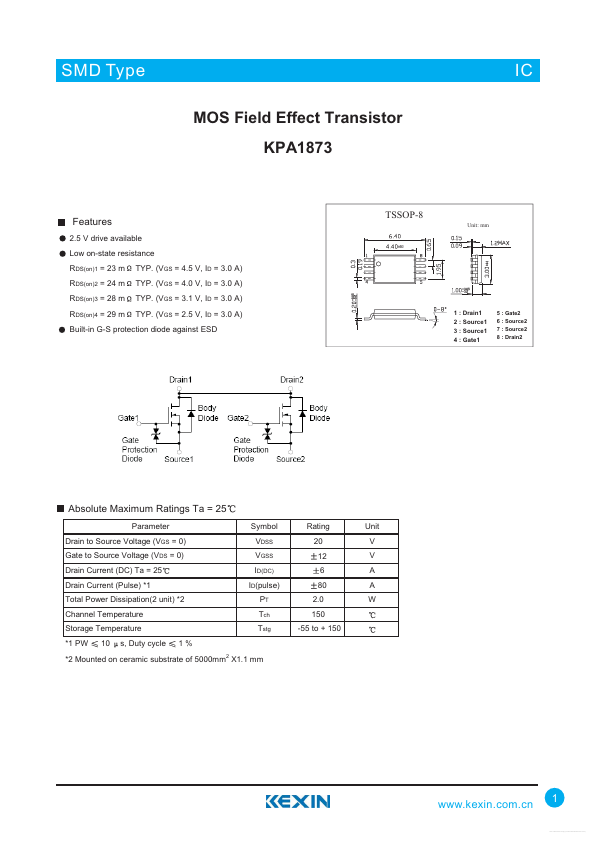
MOS Field Effect Transistor KPA1873 IC IC Features 2.5 V drive available Low on-state resistance RDS(on)1 = 23 m RDS(on)2 = 24 m RDS(on)3 = 28 m RDS(on)4 = 29 m TYP. (VGS = 4.5 V, ID = 3.0 A) TYP. (VGS = 4.0 V, ID = 3.0 A) TYP. (VGS = 3.1 V, ID = 3.0 A) TYP. (VGS = 2.5 V, ID = 3.0 A) TSSOP-8 Unit: mm Built-in G-S protection diode against ESD 1 : Drain1 2 : Source1 3 : Source1 4 : Gate1 5 : Gate2 6 : Source2 7 : Source2 8 : Drain2 Absolute Maximum Ratings Ta = 25 Parameter Drain to Source Voltage (VGS = 0) Gate to Source Voltage (VDS = 0) Drain Current (DC) Ta = 25 Drain Current (Pulse) *1 Total Power Dissipation(2 unit) *2 Channel Temperature Storage Temperature *1 PW 10 s, Duty cycle 1% Symbol VDSS VGSS ID(DC) ID(pulse) PT Tch Tstg Rating 20 12 6 80 2.
Published: |