GAL20LV8
Overview
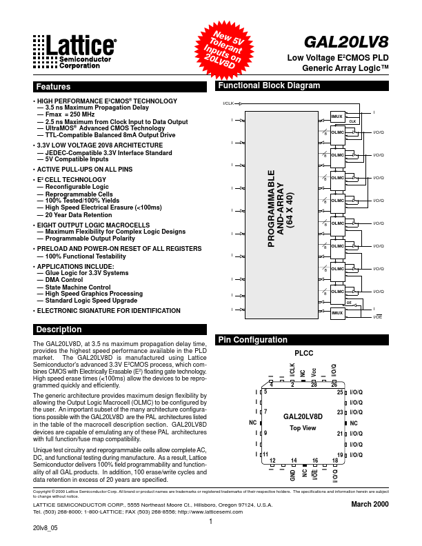
The GAL20LV8D, at 3.5 ns maximum propagation delay time, provides the highest speed performance available in the PLD market. The GAL20LV8D is manufactured using Lattice Semiconductor's advanced 3.3V E2CMOS process, which combines CMOS with Electrically Erasable (E2) floating gate technology.
- HIGH PERFORMANCE E2CMOS® TECHNOLOGY - 3.5 ns Maximum Propagation Delay - Fmax = 250 MHz - 2.5 ns Maximum from Clock Input to Data Output - UltraMOS® Advanced CMOS Technology - TTL-Compatible Balanced 8mA Output Drive
- 3.3V LOW VOLTAGE 20V8 ARCHITECTURE - JEDEC-Compatible 3.3V Interface Standard - 5V Compatible Inputs
- ACTIVE PULL-UPS ON ALL PINS
- E2 CELL TECHNOLOGY - Reconfigurable Logic - Reprogrammable Cells - 100% Tested/100% Yields - High Speed Electrical Erasure (<100ms) - 20 Year Data Retention
- EIGHT OUTPUT LOGIC MACROCELLS - Maximum Flexibility for Complex Logic Designs - Programmable Output Polarity
- PRELOAD AND POWER-ON RESET OF ALL REGISTERS - 100% Functional Testability