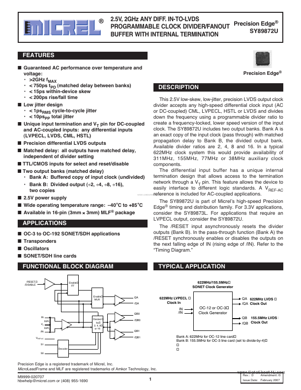
SY89872U Overview
Key Features
- Guaranteed AC performance over temperature and Precision Edge® voltage
- < 750ps tPD (matched delay between banks) DESCRIPTION
- < 15ps within-device skew
- < 200ps rise/fall time This 2.5V low-skew, low-jitter, precision LVDS output clock
- Low jitter design divider accepts any high-speed differential clock input (AC
- < 1psRMS cycle-to-cycle jitter or DC-coupled) CML, LVPECL, HSTL or LVDS and divides
- < 10psPP total jitter down the frequency using a programmable divider ratio to create a frequency-locked, lower speed version of the input
- Precision differential LVDS outputs Available divider ratios are 2, 4, 8 and
- In a typical
- TTL/CMOS inputs for select and reset/disable components. The differential input buffer has a unique internal