MTD2N50E - TMOS POWER FET 2.0 AMPERES 500 VOLTS RDS(on) = 3.6 OHM
Motorola Semiconductor (now NXP Semiconductors)
Key Features
would maintain a value of unity regardless of the switching speed. The circuit used to obtain the data is constructed to minimize common inductance in the drain and gate circuit loops and is believed readily achievable with board mounted components. Most power electronic loads are inductive; the data in the figure is taken with a resistive load, which approximates an optimally snubbed inductive load. Power MOSFETs may be safely operated into an inductive load; however, snubbing reduces switching.
TMOS POWER FET 20 AMPERES 60 VOLTS RDS(on) = 0.080 OHM
Full PDF Text Transcription (Reference)
The following content is an automatically extracted verbatim text
from the original manufacturer datasheet and is provided for reference purposes only.
View original datasheet text
MOTOROLA
SEMICONDUCTOR TECHNICAL DATA
Order this document by MTD2N50E/D
™ Data Sheet TMOS E-FET.™ Power Field Effect Transistor DPAK for Surface Mount
Designer's
MTD2N50E
Motorola Preferred Device
N–Channel Enhancement–Mode Silicon Gate
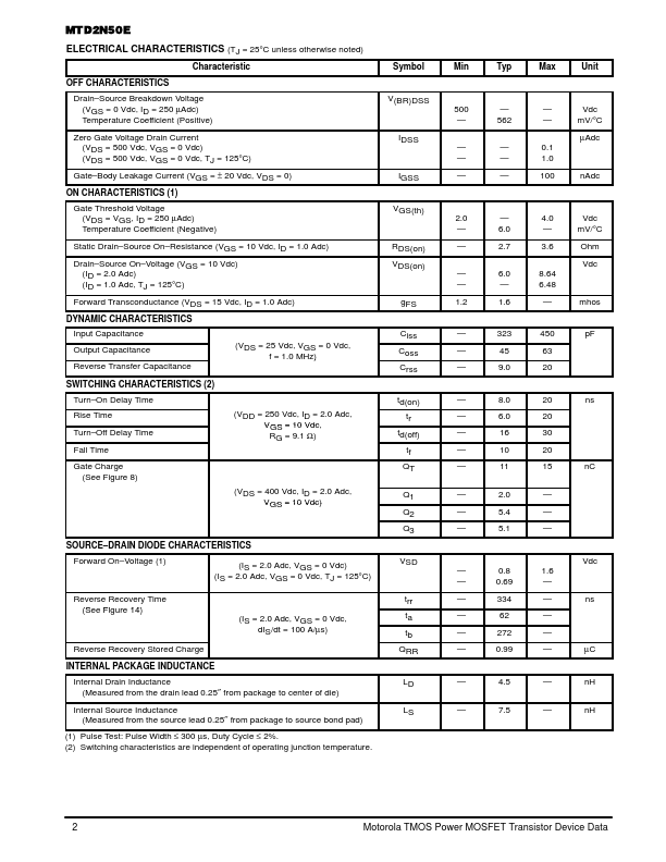
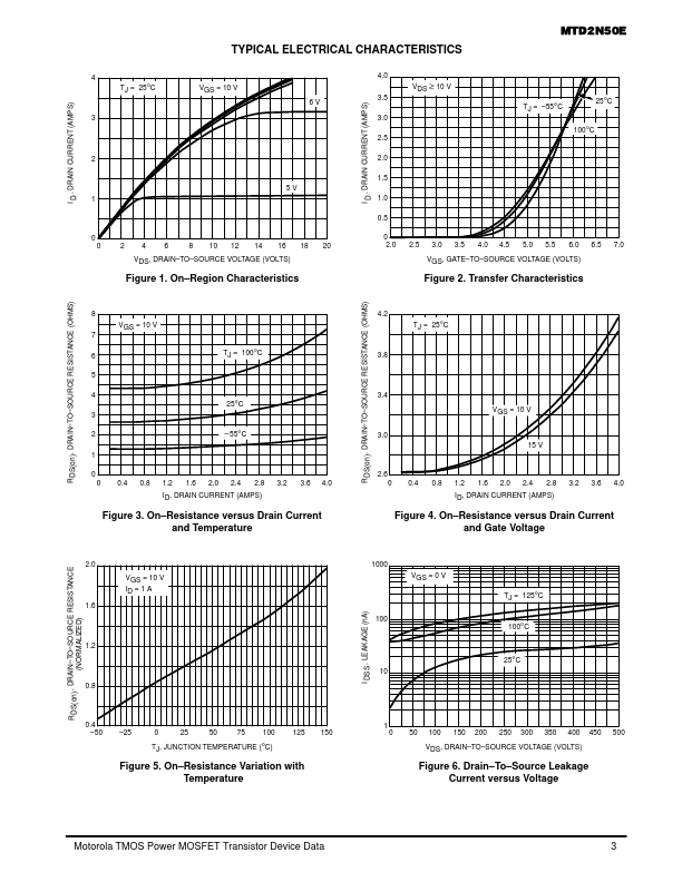
This high voltage MOSFET uses an advanced termination scheme to provide enhanced voltage–blocking capability without degrading performance over time. In addition this advanced TMOS E–FET is designed to withstand high energy in the avalanche and commutation modes. The new energy efficient design also offers a drain–to–source diode with a fast recovery time.