2SK3230C
2SK3230C is MOSFET manufactured by NEC.
DESCRIPTION
The 2SK3230C contains a diode and high resistivity between its gates and sources, for achieving short stability
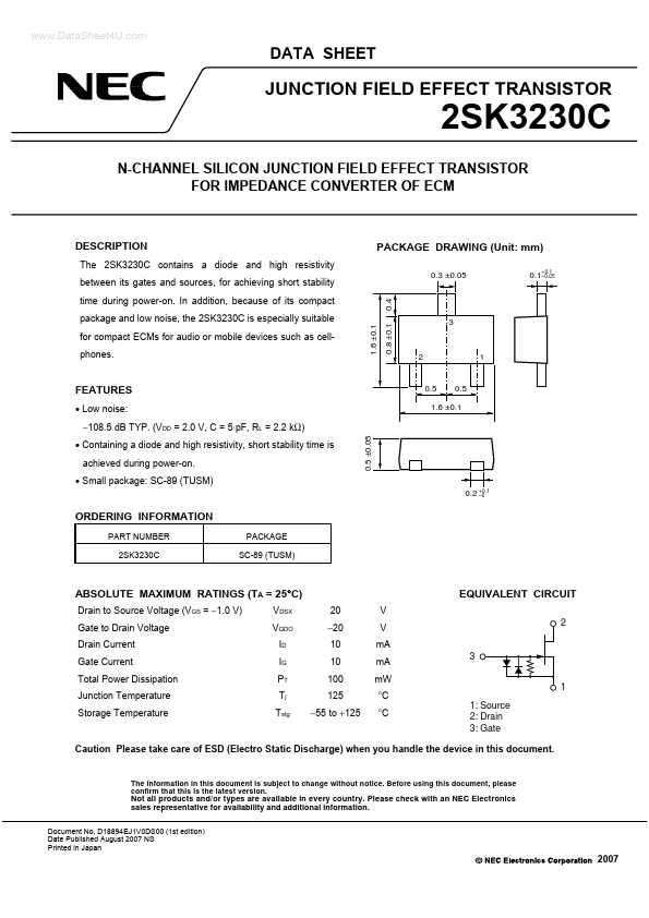
PACKAGE DRAWING (Unit: mm)
0.3 ±0.05
0.1- 0.05
+0.1 time during power-on. In addition, because of its pact
1.6 ±0.1 for pact ECMs for audio or mobile devices such as cellphones.
0.8 ±0.1 package and low noise, the 2SK3230C is especially suitable
FEATURES
- Low noise:
- 108.5 d B TYP. (VDD = 2.0 V, C = 5 p F, RL = 2.2 kΩ)
- Containing a diode and high resistivity, short stability time is achieved during power-on.
- Small package: SC-89 (TUSM)
0.5 ±0.05
1.6 ±0.1
0.2 +0.1
- 0
ORDERING INFORMATION
PART NUMBER 2SK3230C PACKAGE SC-89 (TUSM)
ABSOLUTE MAXIMUM RATINGS (TA = 25°C)
Drain to Source Voltage (VGS =
- 1.0 V) Gate to Drain Voltage Drain Current Gate Current Total Power Dissipation Junction Temperature Storage Temperature VDSX VGDO ID IG PT Tj Tstg 20
- 20 10 10 100 125
- 55 to +125 V V m A m A m W °C °C
EQUIVALENT CIRCUIT
3 1 1: Source 2: Drain 3: Gate
Caution Please take care of ESD (Electro Static Discharge) when you handle the device in this document.
The information in this document is subject to change without notice. Before using this document, please confirm that this is the latest version.
Not all products and/or types are available in every country. Please check with an NEC Electronics sales representative for availability and additional information.
Document No. D18894EJ1V0DS00 (1st edition) Date Published August 2007 NS Printed in Japan
ELECTRICAL CHARACTERISTICS (TA = 25°C)
CHARACTERISTICS Zero Gate Voltage Drain Cut-off Current Gate Cut-off Voltage Forward Transfer Admittance SYMBOL IDSS VGS(off) | yfs1 | | yfs2 | Input Capacitance Voltage Gain Ciss GV TEST CONDITIONS VDS = 2.0 V, VGS = 0 V VDS = 2.0 V, ID = 1.0 μA VDS = 2.0 V, ID = 30 μA, f = 1.0 k Hz VDS = 2.0 V, VGS = 0 V, f = 1.0 k Hz VDS = 2.0 V, VGS = 0 V, f = 1.0 MHz VDD = 2.0 V, C = 5 p F, RL = 2.2 kΩ, VIN = 10 m V, f = 1 k Hz...